Si deseas distinguir tus productos, servicios o ambos de los de otra empresa, es posible que necesites una marca o nombre comercial. Descubre qué son, en qué consiste su procedimiento de registro y qué implica.

Información sobre los plazos de presentación de solicitudes de transformación de marcas de la Unión Europea en marca nacional española. Más información


Si tienes un nuevo dispositivo, producto o procedimiento que resuelva un problema técnico o tenga una ventaja práctica, existen distintas formas de protegerlo en España y en otros países. Descubre cómo hacerlo.

¿Tu innovación reside en la estética, la ornamentación o la apariencia de tu producto? Protégela mediante un diseño industrial. Descubre qué derechos confiere el registro y cómo realizar la tramitación.

Las indicaciones geográficas protegen el nombre de un producto originario de una zona geográfica, a la cual le debe una determinada calidad, reputación u otra característica. Descubre qué son, en qué consiste su procedimiento de registro y qué beneficios conceden.

Las patentes publicadas en todo el mundo son una valiosa fuente de información científica, técnica y comercial.

Si eres emprendedor/a o una empresa y quieres potenciar y mejorar la rentabilidad de tu negocio protegiendo de forma adecuada los activos intangibles de tu organización, en este espacio encontrarás lo necesario.


 224
resultados
224
resultados
 Última actualización
23/10/2026 [09:45:00]
Última actualización
23/10/2026 [09:45:00]


 Resultados 200 a 224 de 224
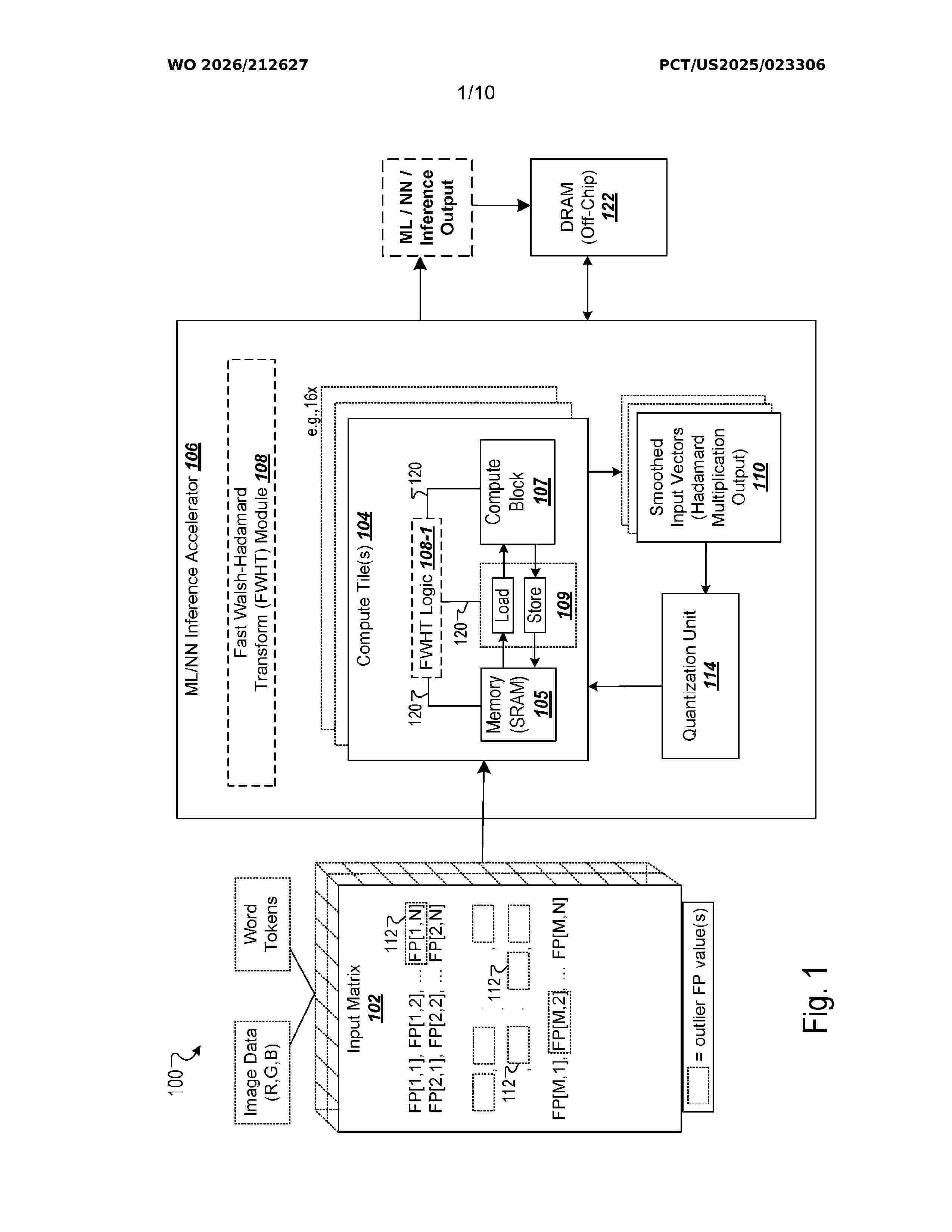
Resumen de: WO2026212627A1
Methods and systems, including computer-readable media, are described for efficient computation of Fast Walsh-Hadamard Transforms on an integrated circuit. The circuit receives an input matrix with floating-point (FP) values for processing at a neural network layer. A Hadamard multiplication output is computed from the FP values using a Hadamard identity matrix. For example, the circuit obtains an input vector of the input matrix. At a first iteration, a first output is computed from vector-matrix operations performed on values of the input vector and a first sub-matrix derived from the Hadamard identity matrix. At a second iteration, a second output is computed from vector-matrix operations performed on the first output and a second sub-matrix derived from the Hadamard identity matrix. A result is computed from a divide-by-2 operation performed on the second output computed at the second iteration. The Hadamard multiplication output is computed using the result of the divide-by-2 operation.

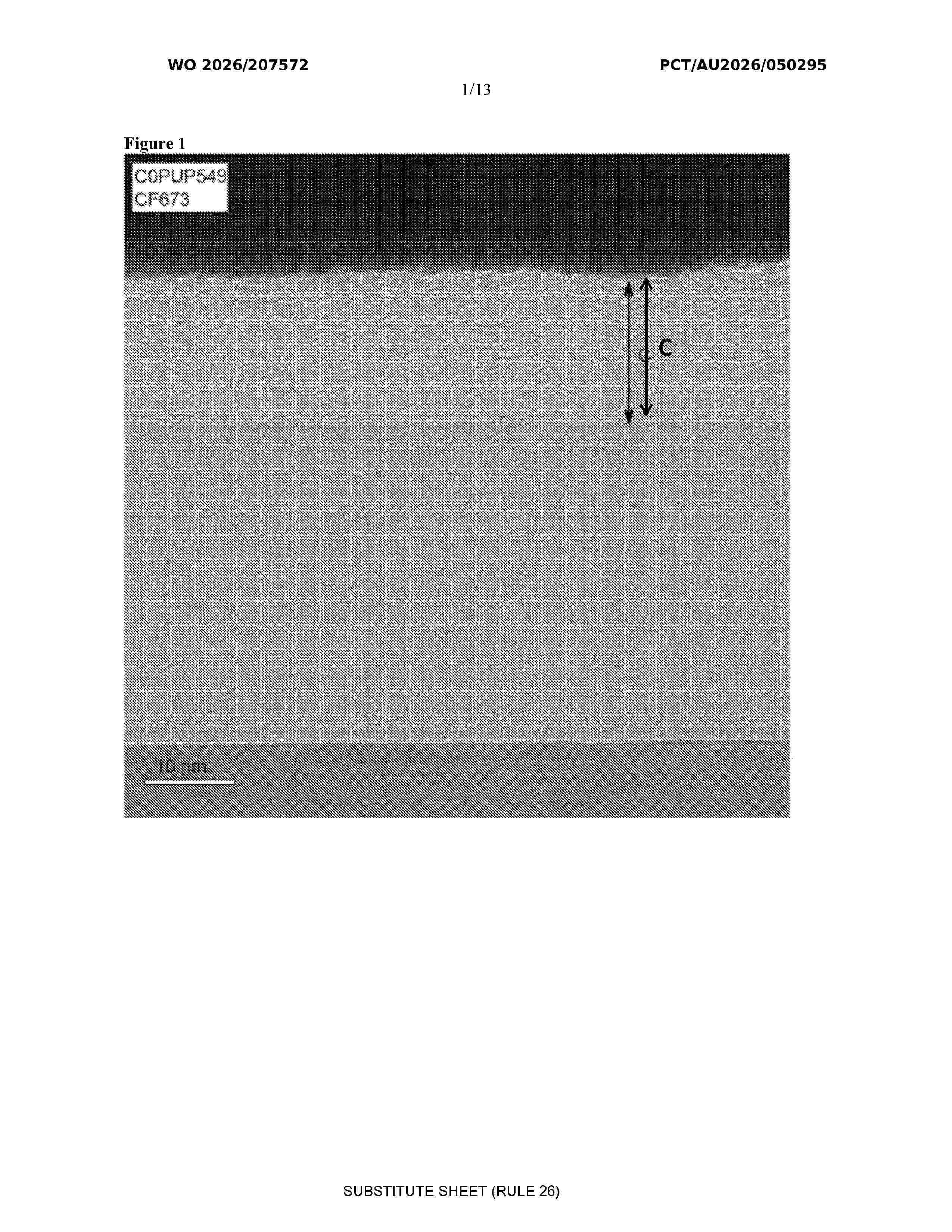
Resumen de: WO2026207572A1
The present invention relates to spin-based logic devices, spintronics, spin quantum devices and new carbon based materials and films for use in same.
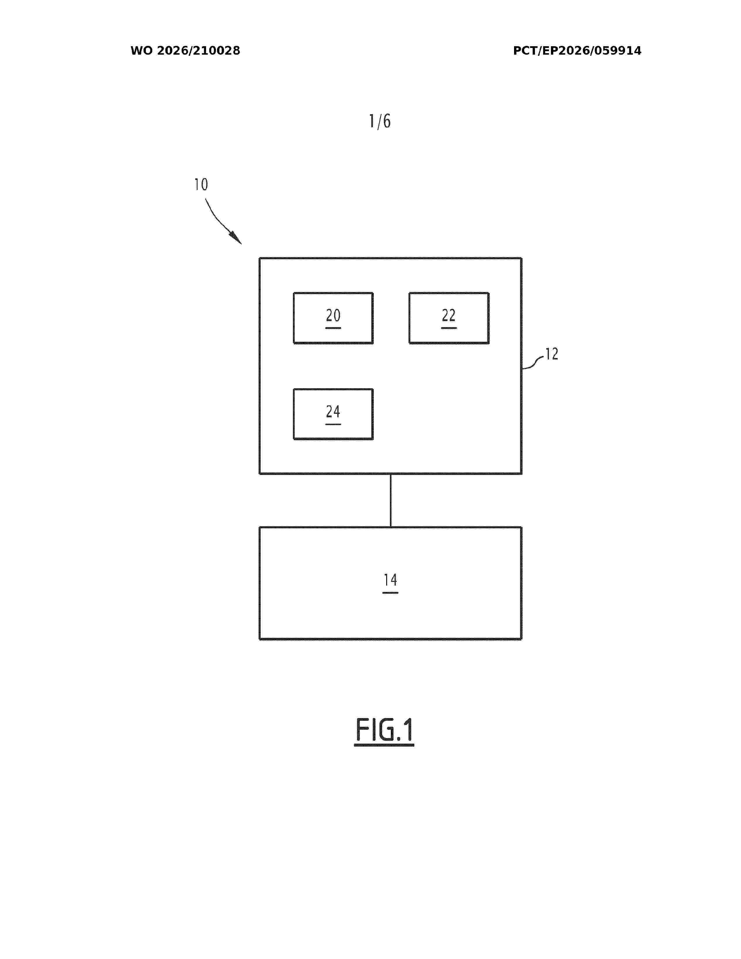
Resumen de: WO2026210028A1
The invention concerns a method for providing rounds of error corrections for a quantum error correction code comprising the following steps: - initializing a quantum register with N data qubits and a number R of sets of K ancilla qubits, - encoding logical information on the N data qubits, - performing R cycles of operations on the quantum register, each cycle of operations comprising entangling gates between part of the N data qubits with part of a distinct set of K ancilla qubits, and - obtaining measurements from the N data qubits and from each of the R sets, each measurement being the result of a quantum projection operation applied on the considered qubit and of the readout of the quantum projection, the measurements obtained from the R sets enabling carrying out R rounds of error corrections on the measurements obtained from the N data qubits.
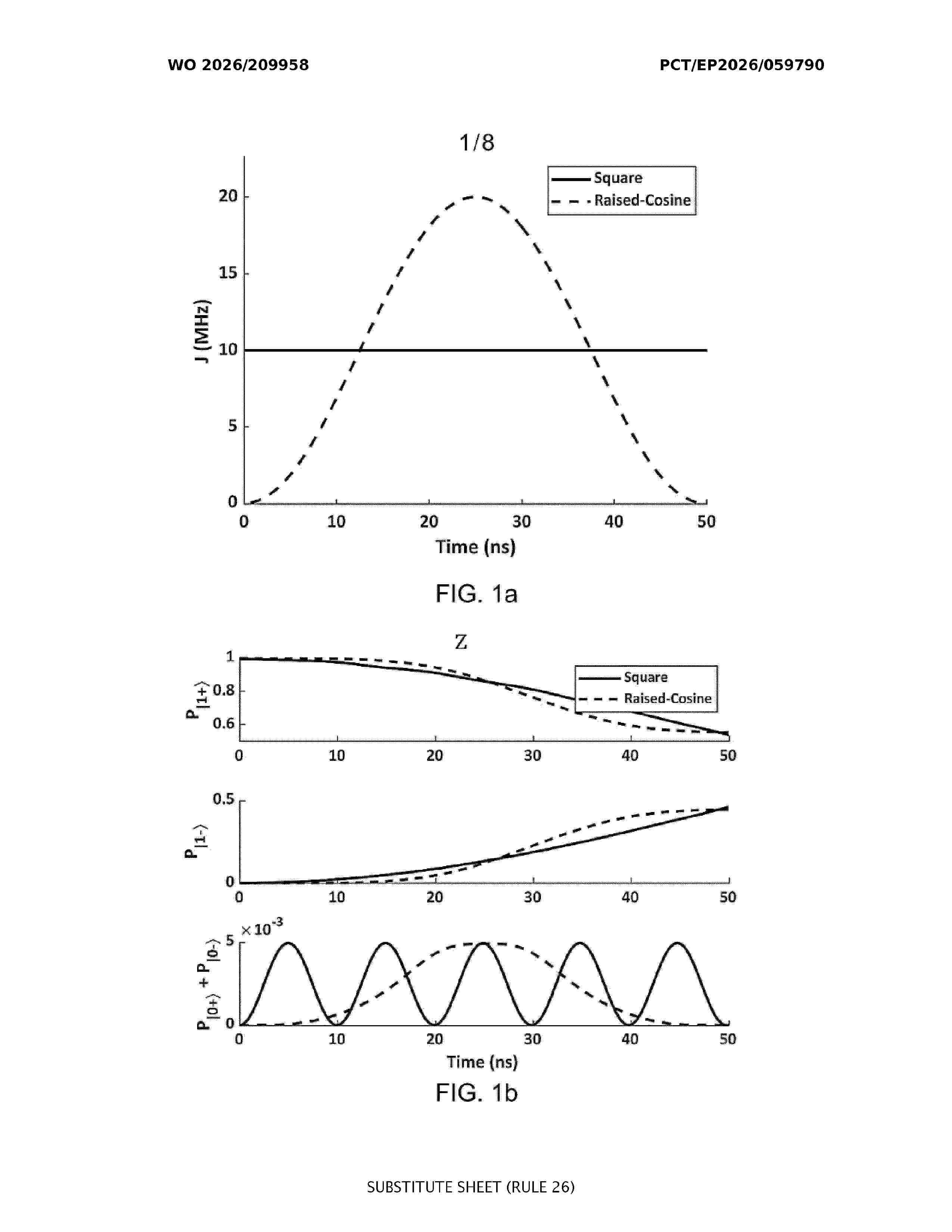
Resumen de: WO2026209958A1
The invention provides a method for driving a quantum system comprising at least two qubits coupled to one another in a quantum sub-system, the method comprising generating a composite time-varying electromagnetic signal, which is a composition of a time-varying electromagnetic signal and for each oscillation in the quantum sub-system a time delayed version of substantially this time-varying electromagnetic signal, delayed by a customized delay time ���� with respect to the time-varying electromagnetic signal for generating a notch in the composite electromagnetic signal spectrum, and applying the composite electromagnetic signal to the quantum sub-system.
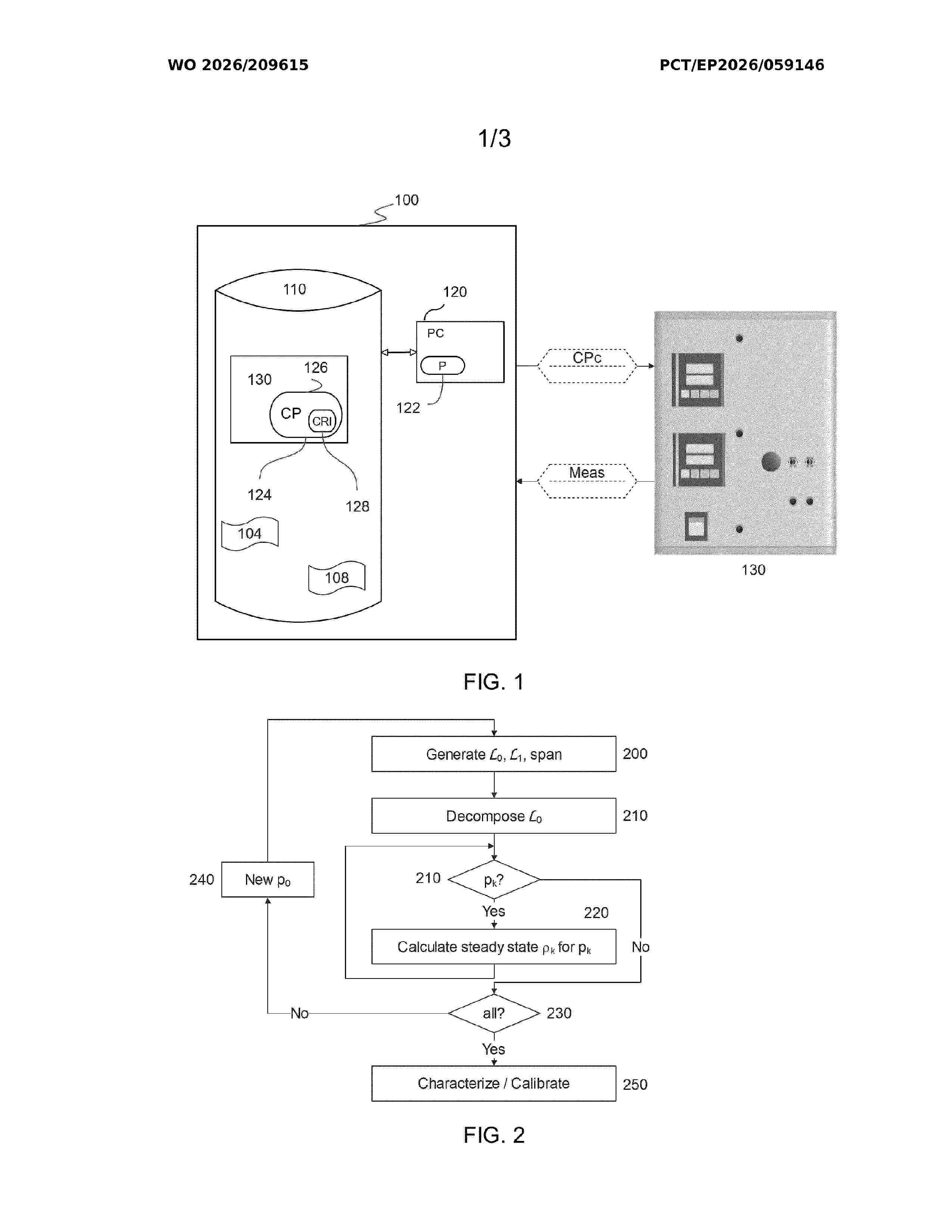
Resumen de: WO2026209615A1
A computer implemented method for calculating a plurality of steady states of an open quantum system which is a physical quantum system being governed by a Lindblad master equation parametrized by a set of parameters p which characterize the physical quantum system and comprise fixed parameters and variable parameters, comprising the following operations: a) based on an initial set of parameters p 0 , reformulating (200) said Linblad master equation in the form £(p) = £ 0 + Δ p £ 1 where p = p 0 + Δ p , £ 0 = £(p 0 ), and £ 1 is a Liouvillian, b) summing the trace superoperator T with a chosen complex coefficient b to £ 0 , to obtain (I), and performing (210) a LU decomposition or an incomplete LU decomposition of (I), after operation b), for each of a plurality of parameters sets {p k } k such that p k = p 0 + Δ k , c) computing (220) a candidate steady state (II) by c1) determining a steady state basis (III), where n is an integer smaller than a chosen maximum number N 0 of basis members, in which the first member is derived from b or Δ k , and all basis members respect the condition (IV) or (V) for n>0, using the decomposition from operation a), c2) computing said candidate steady state (VI) for the parameter set p k by determining the set of coefficients {cn}n minimizing the equation (VII), where B = b; 0;...; 0 based on the value of (VIII), returning (II) as the steady state for the parameter set p k , or else storing parameter set p k as a parameter s
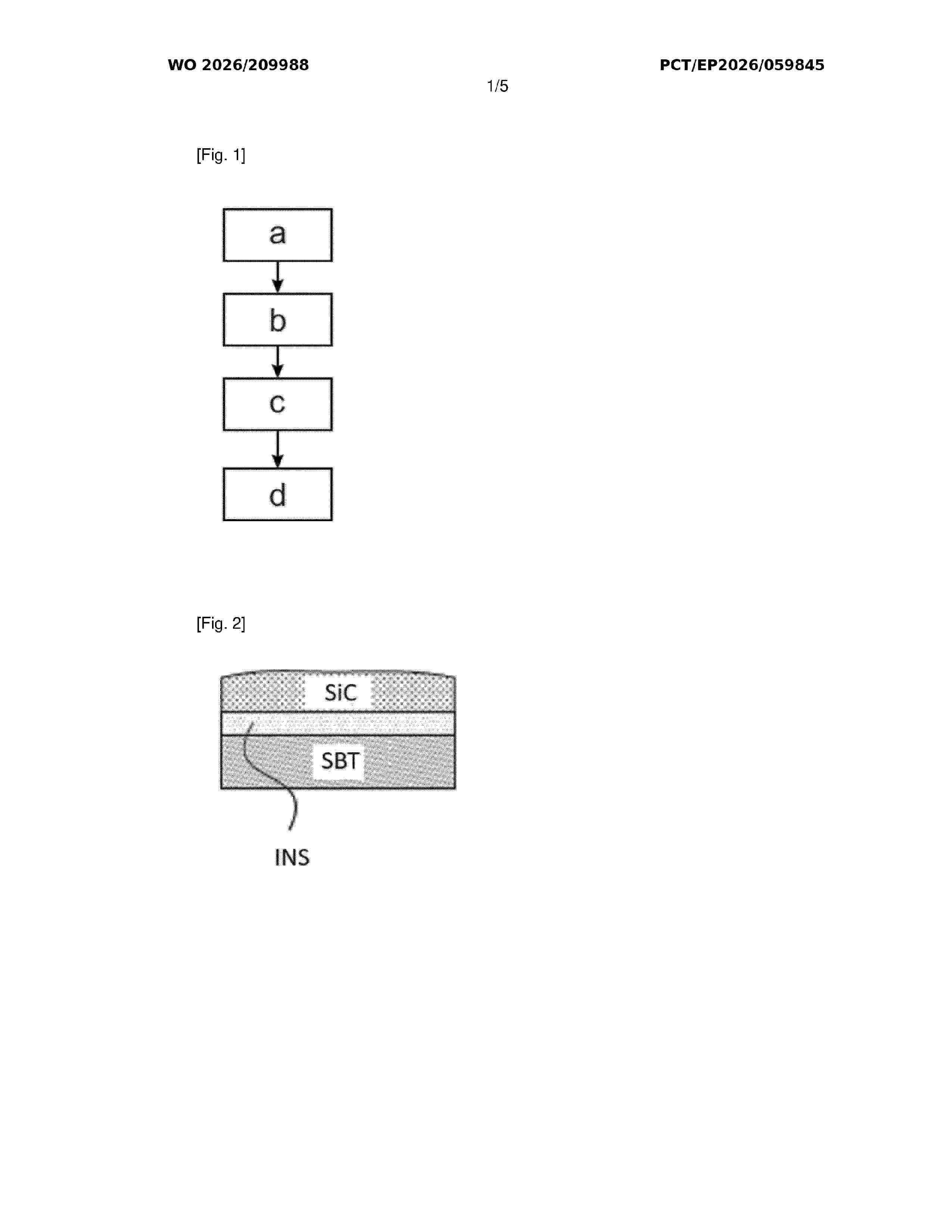
Resumen de: WO2026209988A1
The invention relates to a method for manufacturing a silicon carbide on insulator, said method comprising the following steps: a) providing a substrate, b) providing a silicon carbide structure, at least one of the substrate and of the silicon carbide structure being provided with an electrically insulating layer; c) arranging the silicon carbide structure against the substrate with the electrically insulating layer between them so as to form a contact between them; d) focusing a laser beam towards the electrically insulating layer to weld the silicon carbide structure to the substrate, the laser beam being controlled to define one or several welded areas separated by one or several non-welded areas. The invention also relates to a method for manufacturing SiCOI photonic structures that may contain one or several color centers, from a SiCOI structure obtained with the manufacturing method of the invention.
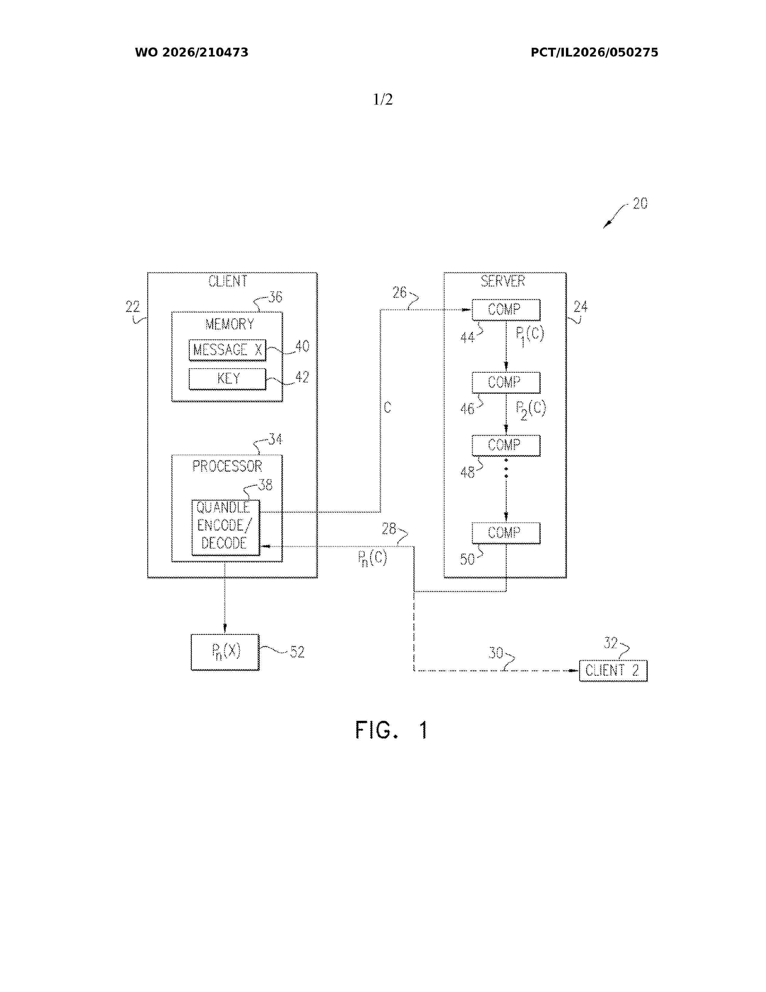
Resumen de: WO2026210473A1
A cryptographic method includes receiving an input tensor, which has a rank of at least one and is an element of a specified quandle. The method includes encrypting the input tensor by performing a first operation of the specified quandle over the input tensor together with an encoding tensor, which is a further element of the specified quandle, to generate an encrypted output tensor. The method includes transmitting the encrypted output tensor to a recipient, wherein the encrypted output tensor is decryptable using the encoding tensor in a second operation of the quandle.
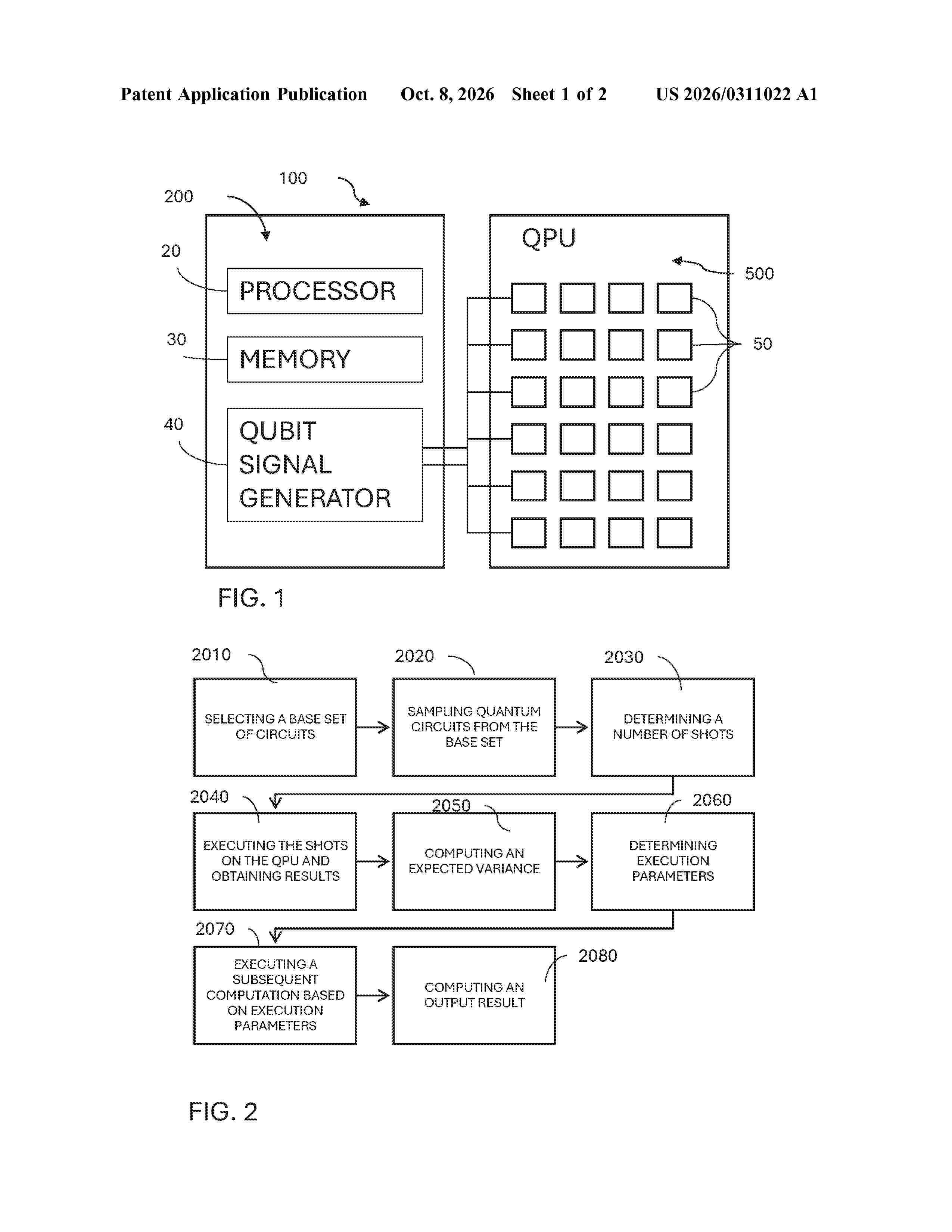
Resumen de: US20260311022A1
A quantum-computer control technique is disclosed for reducing quantum processing unit runtime or a number of executed measurement shots while achieving a target statistical uncertainty of an output result. Quantum circuits are sampled from a base set according to a circuit distribution, and, for each sampled circuit, a number of measurement shots is determined in accordance with a shot distribution and executed on one or more qubits to obtain measurement results. An expected variance of an expectation value estimate is computed based on the measurement results and is based on at least a shot-related variance component and a circuit-to-circuit variance component. Based on the expected variance, one or more execution parameters for a subsequent quantum computation are determined, including a number of circuits, a number of shots, and/or updated distributions, and the subsequent computation is executed accordingly. System, storage-medium, and simulation embodiments are also described.
Resumen de: US20260311026A1
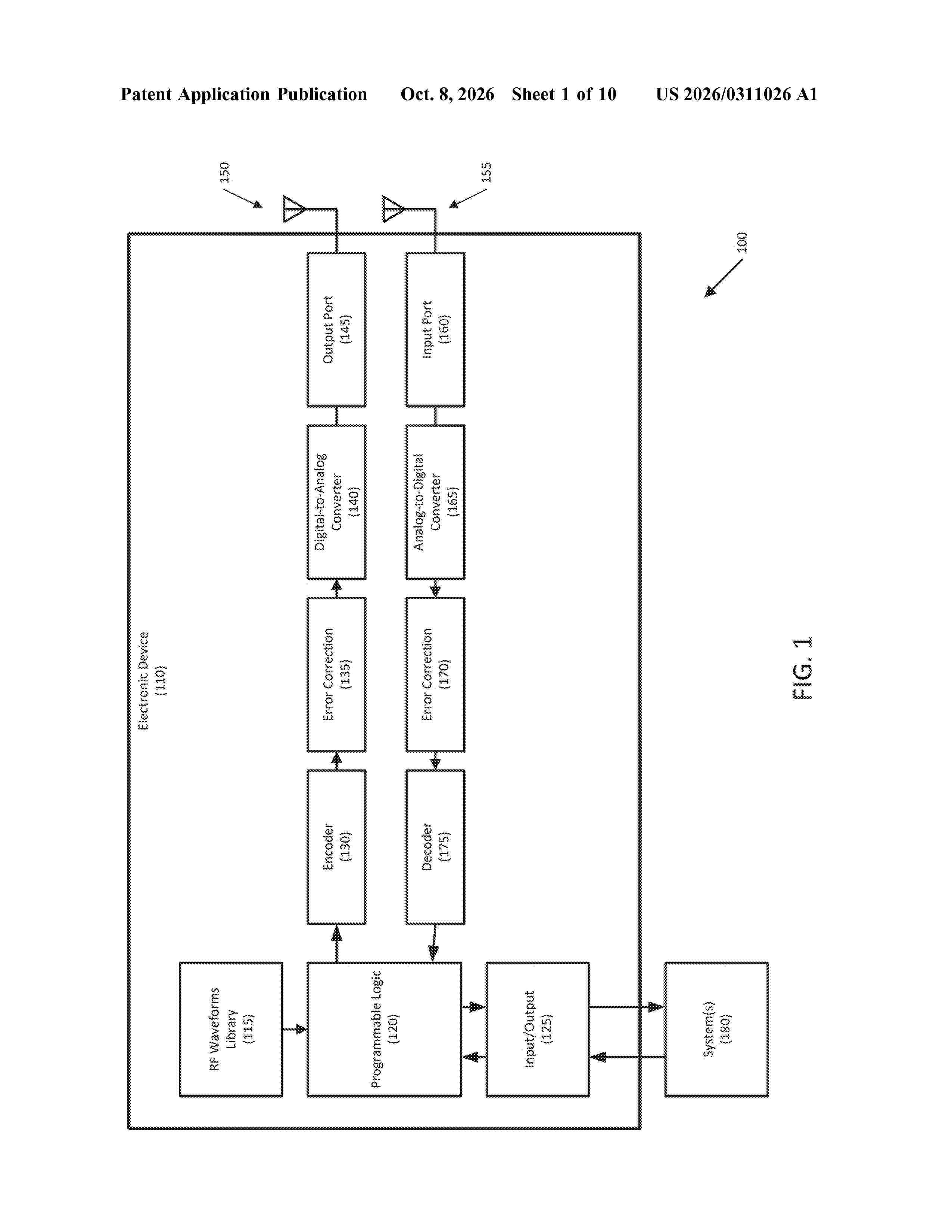
0000 An electronic device may include programmable logic that generates a first digital signal; an encoder that encodes the first digital signal as a positive amplitude and a negative amplitude using a first RF waveform that is selected based on a value of the first digital signal and comprises an initial calibration pulse; an output port that outputs the encoded first analog signal to a second electronic device over a low-latency connection; an input port that receives an encoded second analog signal from the second electronic device over the low-latency connection; a decoder that extracts the encoded second digital signal into a second digital signal by measuring the encoded second digital signal and a received calibration pulse in the encoded second digital signal; and an input/output interface provides the second digital signal to a system that is configured to execute an action based on the second digital signal.
Resumen de: US20260311013A1
0000 The invention introduces a Total Wave structure of the Modified Schrödinger Equation (MSE) that deterministically governs quantum collapse using co-evolving field-specific wave-functions. Unlike conventional quantum mechanics, which treats wavefunction collapse as a postulated or probabilistic phenomenon, this invention models collapse as a structured outcome of wave interference from multiple physical fields—electromagnetic, gravitational, strong nuclear, and weak nuclear—each governed by its own nonlinear MSE. 0000 The system wavefunction Ψ
evolves under the influence of these field-specific observer waves Ψ
Resumen de: WO2026209567A1
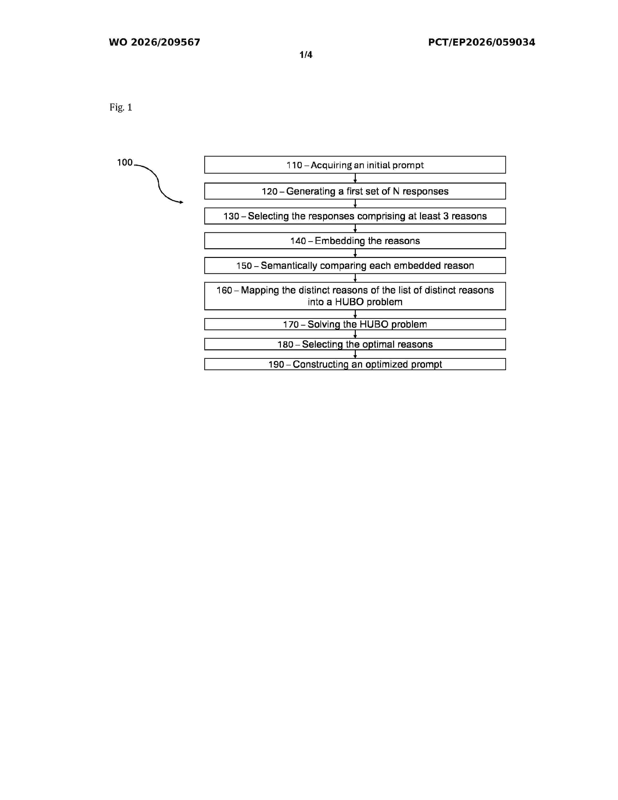
The invention presents a computer-implemented method (100) and system for constructing optimized prompts for large language models. The method (100) involves acquiring an initial prompt from a user, generating multiple responses from the large language model, and selecting responses that contain multiple reasons. These reasons are embedded and semantically compared to create a distinct set. The distinct reasons are then mapped into a higher-order unconstrained binary optimization problem, which captures complex interactions among reasons. The optimization problem is solved using a quantum processing unit, yielding optimal reasons that are used to construct a final prompt. This optimized prompt enhances the reasoning capabilities of large language models by effectively modeling multi-factor dependencies and interactions.
Resumen de: WO2026210061A1
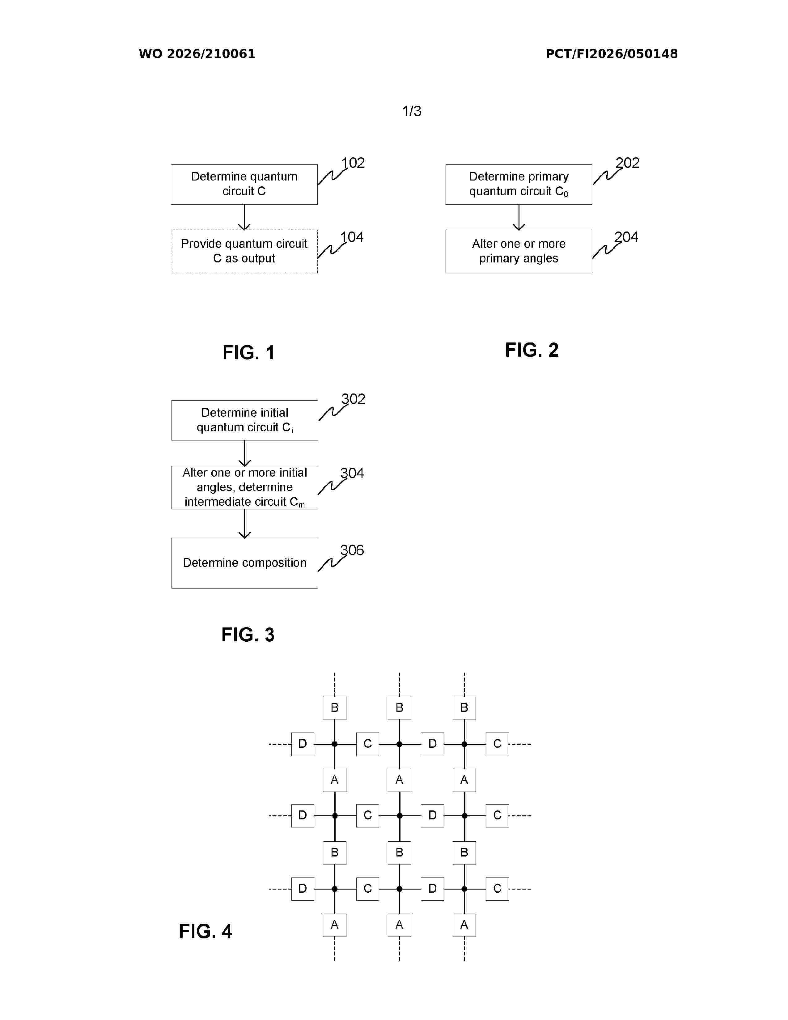
A computer-implemented method for determining a quantum circuit, wherein the method comprises, by utilizing at least a first computing device, determining a quantum circuit C that implements a perturbed unitary transformation Up, wherein the quantum circuit C is determined as corresponding to a quantum circuit obtained by applying a perturbation to a primary quantum circuit Co, wherein the primary quantum circuit Co implements a predetermined unitary transformation U, by altering with selected amount(s) one or more parameters of the primary quantum circuit Co to be applied on the quantum states of the quantum elements, wherein the quantum circuit C is determined such that when the quantum circuit C is executed a plurality of times from a fixed initial quantum state |i) on N quantum elements, a predetermined final quantum state |S) is obtained with probability Pc and a difference |Pc - Pu| is within a selected range, where Pu is a probability of obtaining the final quantum state |S) when executing the primary quantum circuit Co a plurality of times from the fixed initial quantum state |i) on N quantum elements.
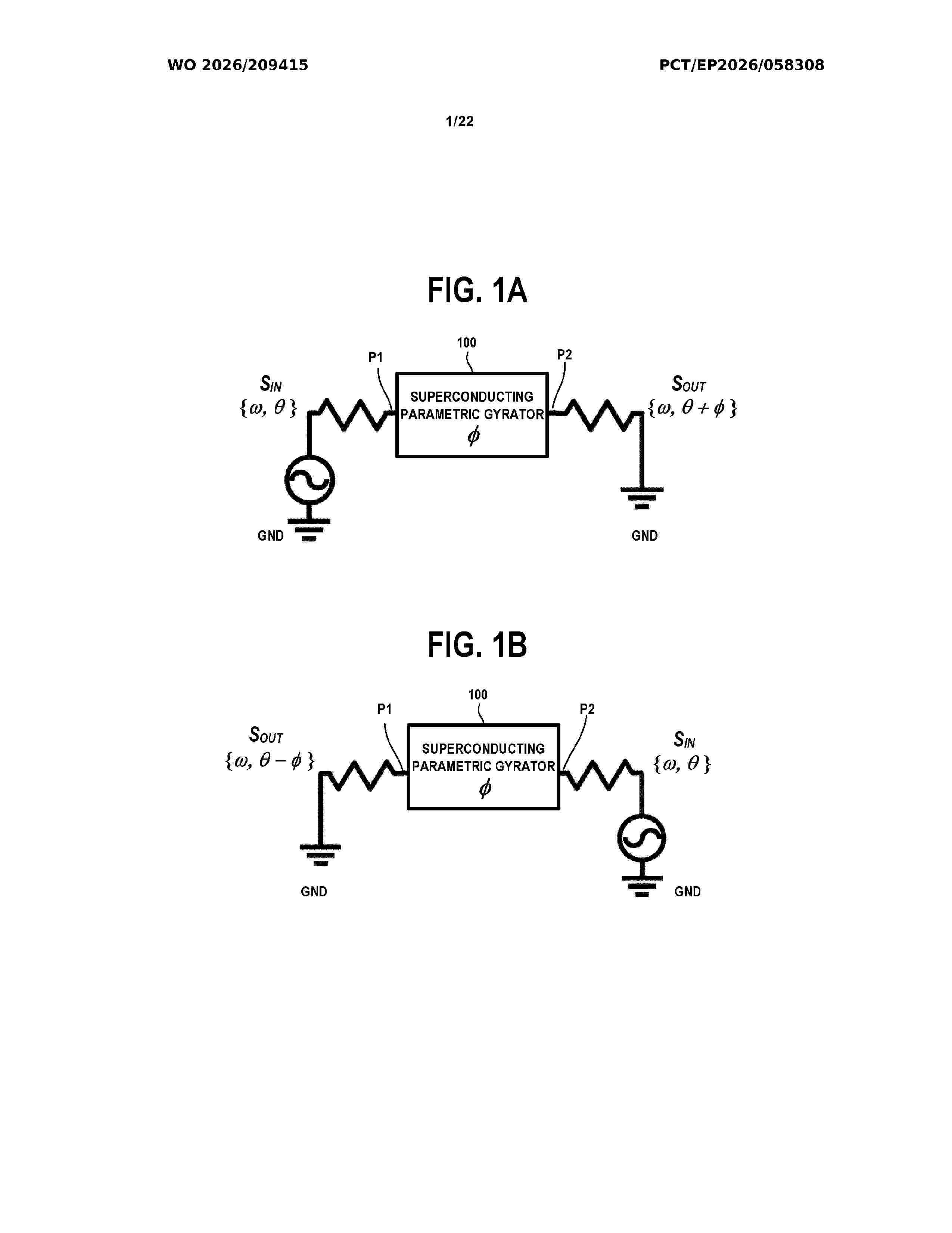
Resumen de: WO2026209415A1
A device comprises a superconducting parametric gyrator circuit comprising a first I/O port, a second I/O port, and a parametric multipole bandpass filter circuit coupled between the first I/O port and the second I/O port. The parametric multipole bandpass filter circuit is responsive to a first control signal and a second control signal, which have a same frequency but different phases, to perform parametric frequency mixing of the first and second control signals with an input signal applied to the first I/O port or the second I/O port, to generate an output signal which has a same frequency as the input signal and a non-reciprocal phase shift based on a phase difference between the first control signal and the second control signal, and based on a direction of propagation of the input signal between the first I/O port and the second I/O port.
Resumen de: WO2026210195A1
A modular, room-temperature photonic quantum computer with AI-driven fault correction, thermal control, and dynamic scalability. A modular quantum computing system is disclosed, operating at room temperature and built from interconnected photonic qubit modules. Each module integrates single-photon sources, optical waveguides, environmental sensors, and a local AI controller. A global artificial intelligence subsystem coordinates real-time error correction, timing synchronization, and dynamic workload balancing using reinforcement learning. The architecture incorporates graphene-based thermal management for passive and predictive heat control, eliminating the need for cryogenic cooling. Modules are hot-swappable, auto-calibrating, and operable in rugged, non-laboratory environments. This system enables scalable, fault-tolerant, high-fidelity quantum computation through a distributed, self-regulating architecture optimized for field deployment.
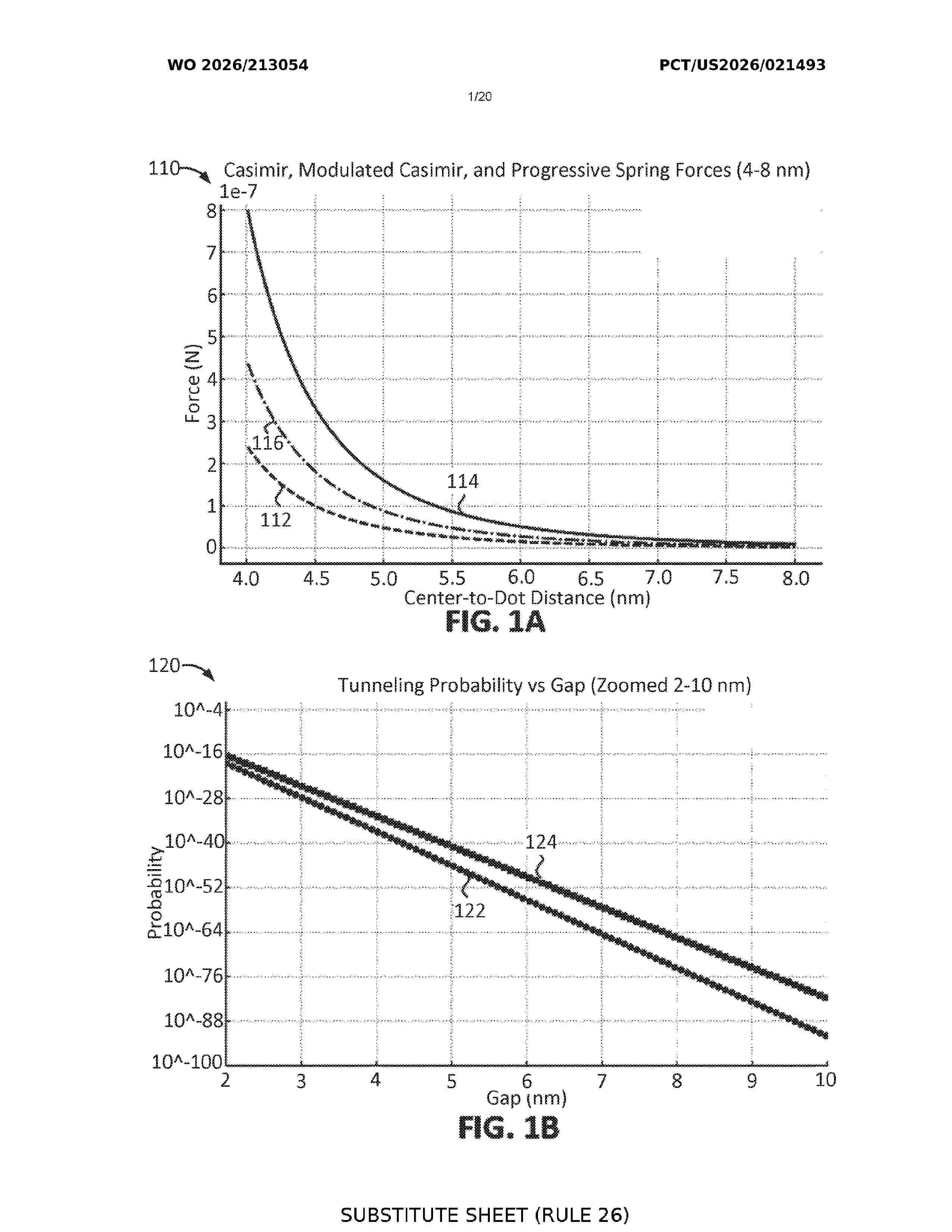
Resumen de: WO2026213054A1
A quantum device includes an actuator including a graphene material and having a proximal end mounted to an actuator anchor; an electrode disposed on a distal end of the actuator; a quantum dot, configured to localize a single electron, the quantum dot and the electrode disposed within a common vacuum to define a tunneling gap; and a quantum dot anchor, comprising the graphene material, disposed in a same plane as the quantum dot relative to the electrode. The quantum device may include a modulator configured to emit electromagnetic signaling within a particular frequency range. The graphene material is tuned to increase a Casimir force between the electrode and the quantum dot anchor in response to the electromagnetic signaling. The increased Casimir force causes the actuator to deform to bring the electrode within an electron tunneling range of the quantum dot, or lowers a tunneling barrier on a static electrode.
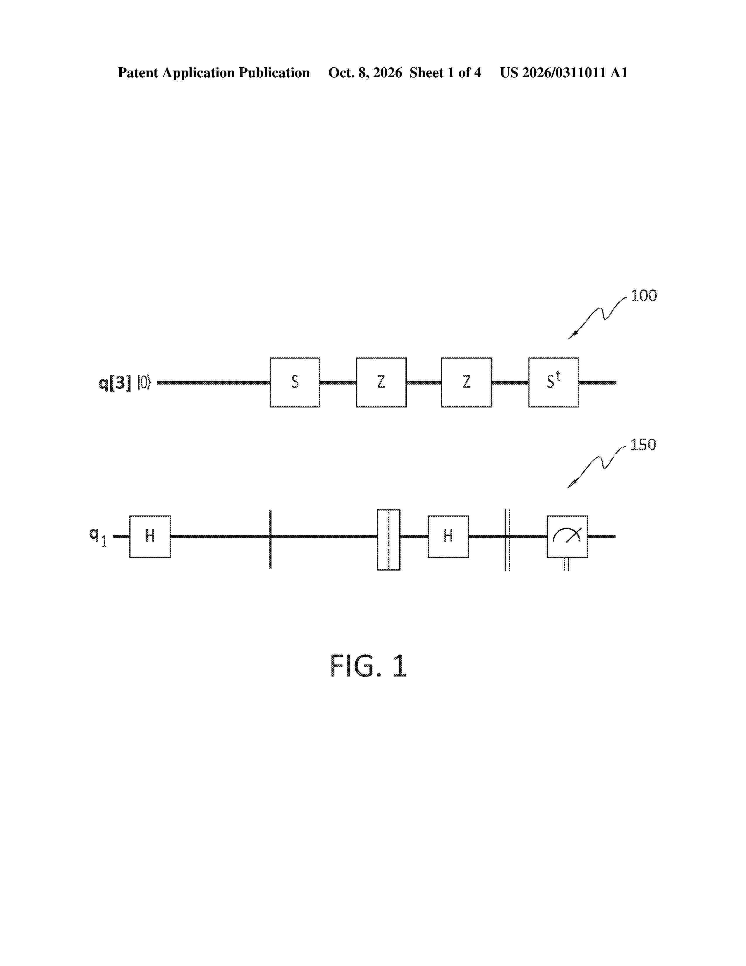
Resumen de: US20260311011A1
One example method includes receiving a quantum circuit for execution on a QPU (quantum processing unit), assigning qubits of the QPU to logical qubits of the quantum circuit, automatically adding, to the quantum circuit, one or more remaining qubits of the QPU as canary qubits, transmitting the quantum circuit to the QPU for execution, and transmitting one or more gate sequences to the QPU for execution by the canary qubits, and execution of the quantum circuit and execution of the gate sequences collectively comprise a single shot.
Resumen de: US20260311012A1
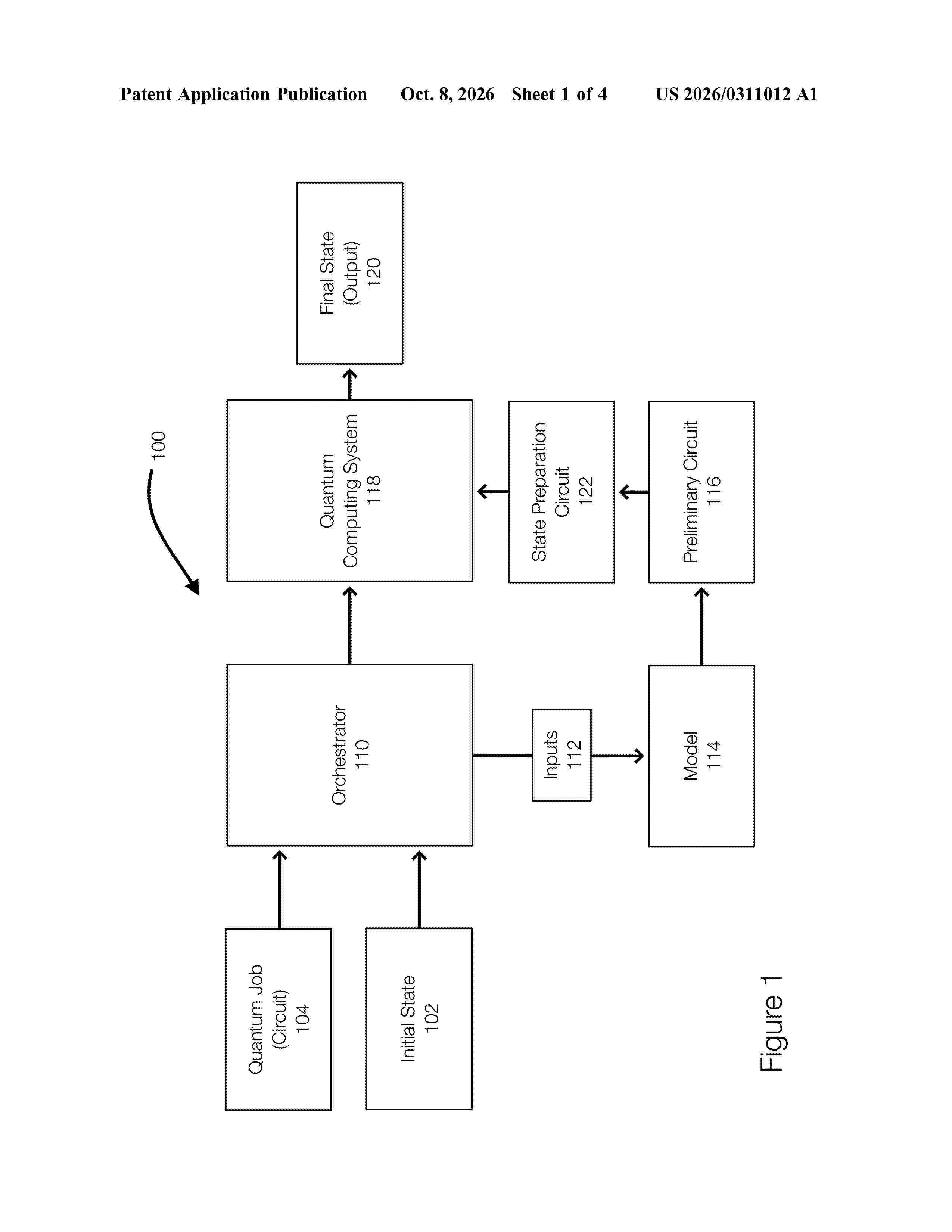
Reinforcement learning with noise emulation to prepare quantum states is disclosed. Using a dataset of random states, a model is trained to generate a preliminary circuit. A state preparation circuit, which is an inverse of the preliminary circuit can be used to place a quantum computing system in a desired initial state. Quantum jobs can be executed after the initial state is prepared.
Resumen de: US20260311020A1
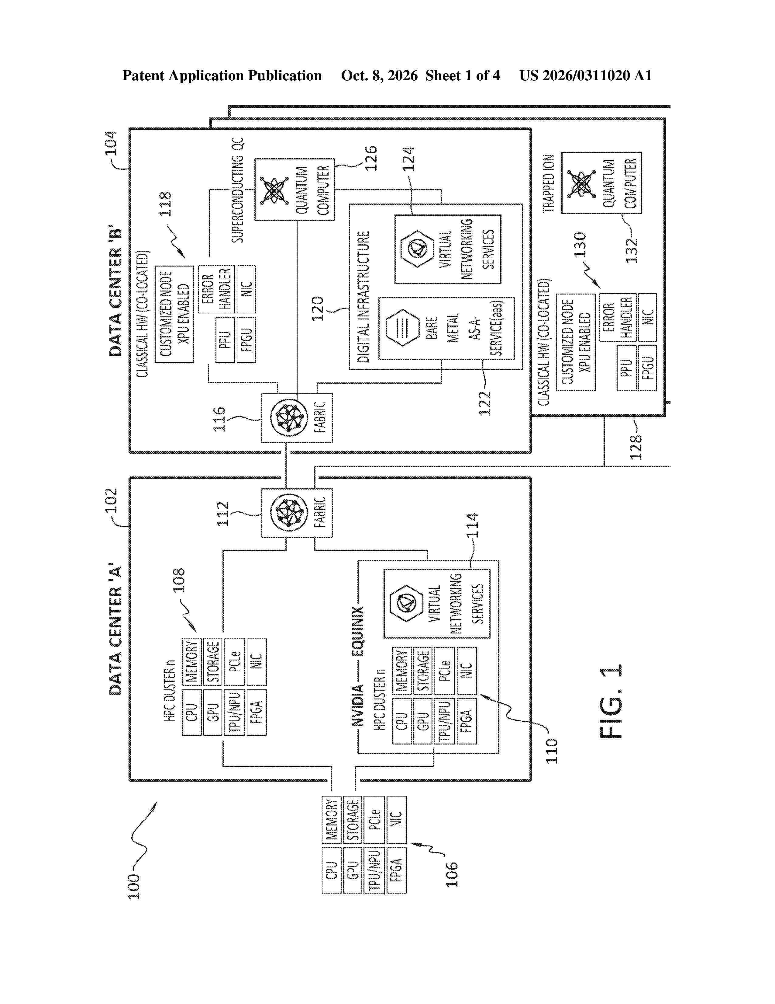
0000 One example method is directed to quantum job orchestration, and includes obtaining, by an orchestration instance, telemetry from respective control planes associated with one or more QPUs (quantum processing units), providing the telemetry as input to an ML (machine learning) model of the orchestration instance, using the ML model to perform an inferencing process whose output is a profile that comprises information usable to make an orchestration decision for a job, based on the profile, orchestrating the job to a particular one of the QPUs, and broadcasting the profile to one or more other orchestration instances.
Resumen de: WO2026208632A1
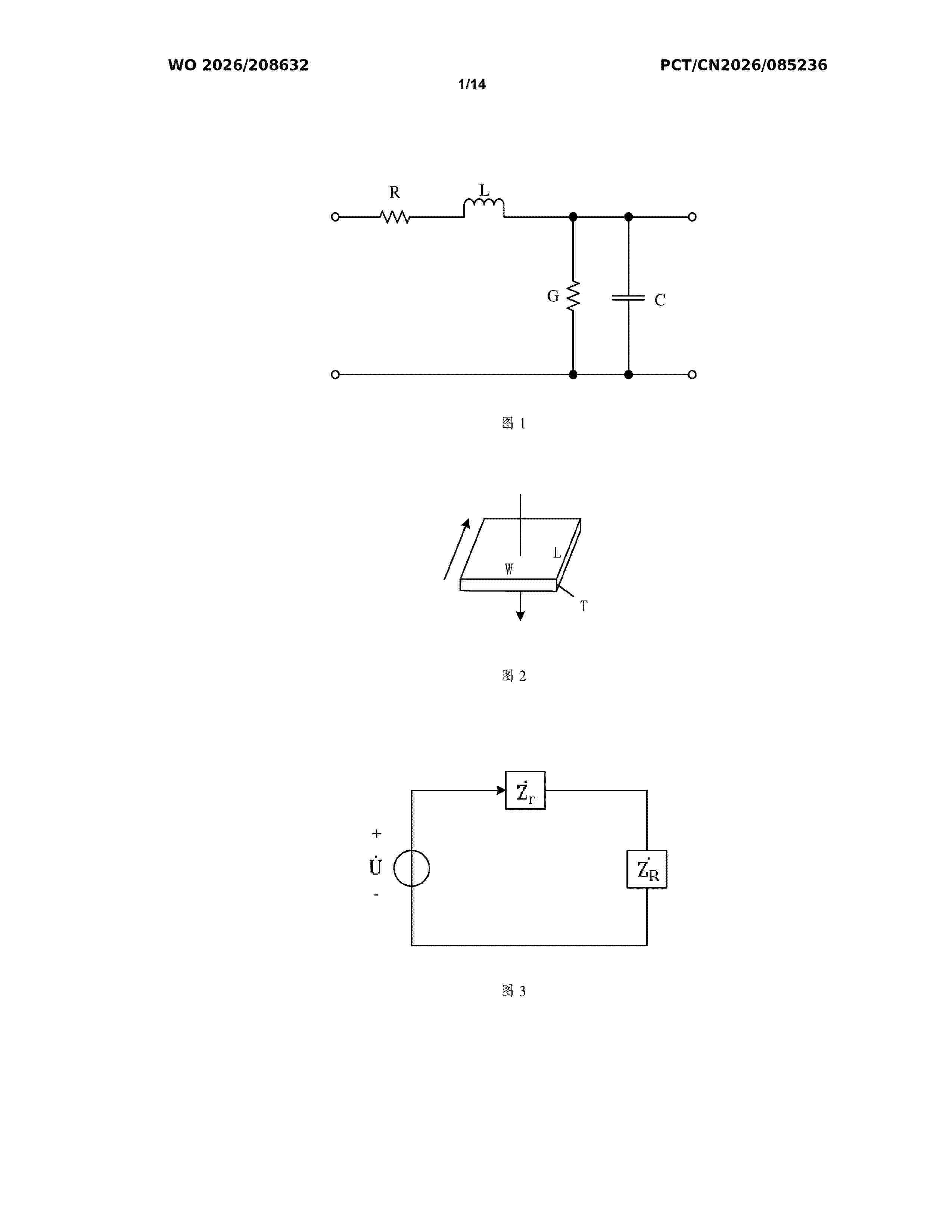
Embodiments of the present application relate to the technical field of quantum computing, and provide a superconducting quantum chip and a superconducting quantum computer. The superconducting quantum chip comprises a transmission line, a manipulation line, and a qubit. The transmission line may include an input line, the input line is connected to the manipulation line, and the manipulation line is electromagnetically coupled to the qubit. The input line is used for transmitting a first microwave signal sent by a microwave device to the manipulation line, and the manipulation line is used for changing the state of the qubit on the basis of the first microwave signal so as to implement quantum computing, wherein the difference between the impedance of the transmission line and the impedance of the microwave device is less than a preset value, and the impedance of the transmission line is determined on the basis of the kinetic inductance, geometric inductance, and capacitance of the transmission line. The introduction of kinetic inductance can increase the overall inductance of the transmission line, thereby increasing the impedance of the transmission line, and reducing the difference between the impedance of the transmission line and the impedance of the microwave device; when such a transmission line is used as the input line, the reflection of the first microwave signal transmitted on the input line can be reduced, thereby improving the accuracy of qubit manipulation.
Resumen de: US20260311017A1
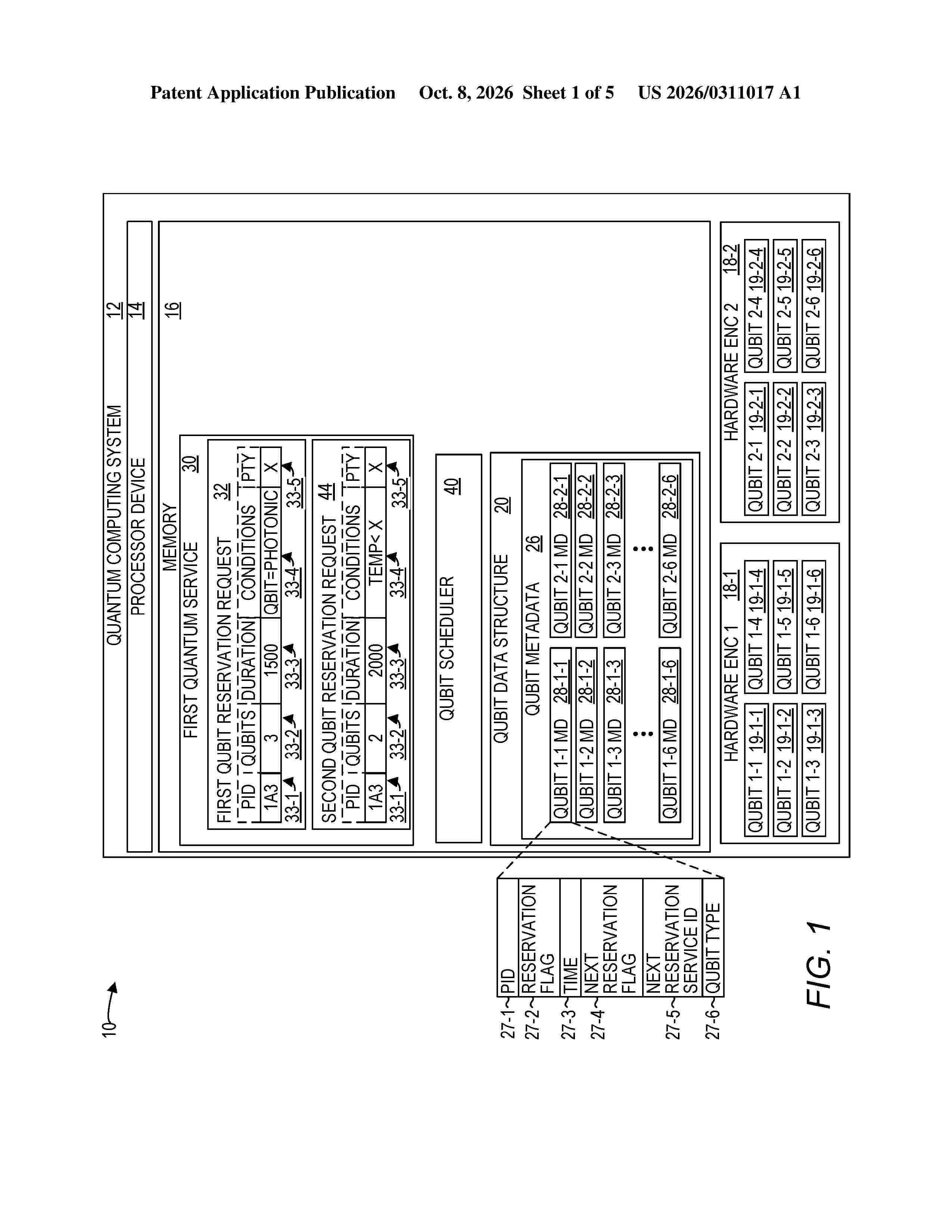
0000 A quantum computing system receives a first qubit reservation request from a first quantum service, the first qubit reservation request identifying a first quantity of qubits. A first set of qubits equal in number to the first quantity of qubits is determined based on a qubit data structure that identifies a first plurality of qubits. The qubit data structure is altered to reserve the first set of qubits for the first quantum service. Qubit reservation information that identifies the first set of qubits is sent to the first quantum service.
Resumen de: US20260311018A1
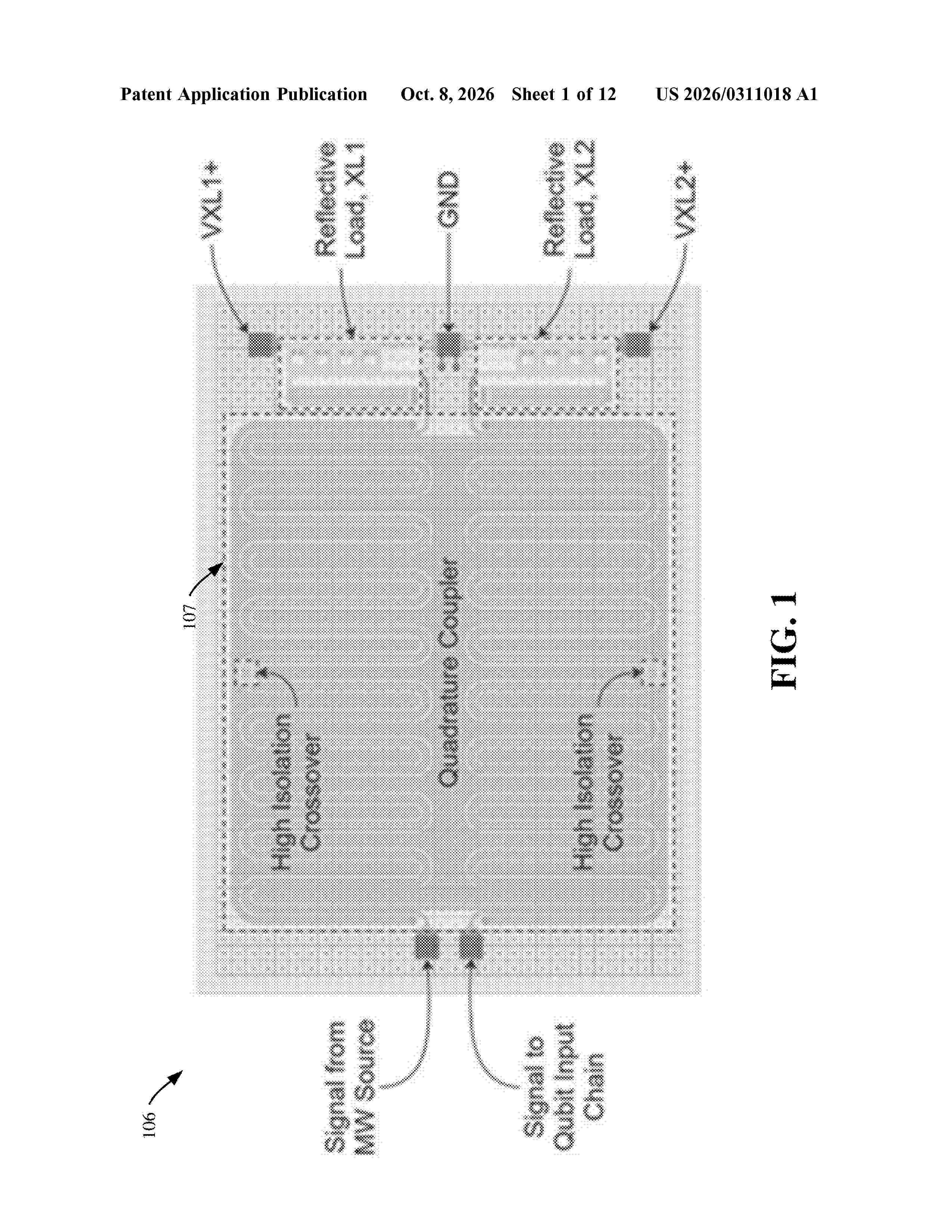
The technology described herein is directed towards a superconducting phase shifter with phase shift controlled via radio-frequency superconducting quantum interference devices (RF-SQUIDs). The phase shifter incorporates a quadrature hybrid coupler that divides an incoming microwave signal into microwave signals to reflective loads of the phase shifter. The inductances of the reflective loads are tuned by voltages/current levels applied to respective control lines coupled to RF-SQUID sets inductively coupled to inductors of the reflective loads. The reflected instances constructively interfere to output a finely (voltage) controlled phase-shifted signal. In one implementation, the superconducting phase shifter can be monolithically integrated on the same chip at the qubits. The superconducting phase shifter can be controlled by a classical computing device that can monitor a qubit's phase-related information, can adjust the phase control system, via the superconducting phase shifter in real time based on any detected phase drift and/or phase noise.
Resumen de: US20260311027A1
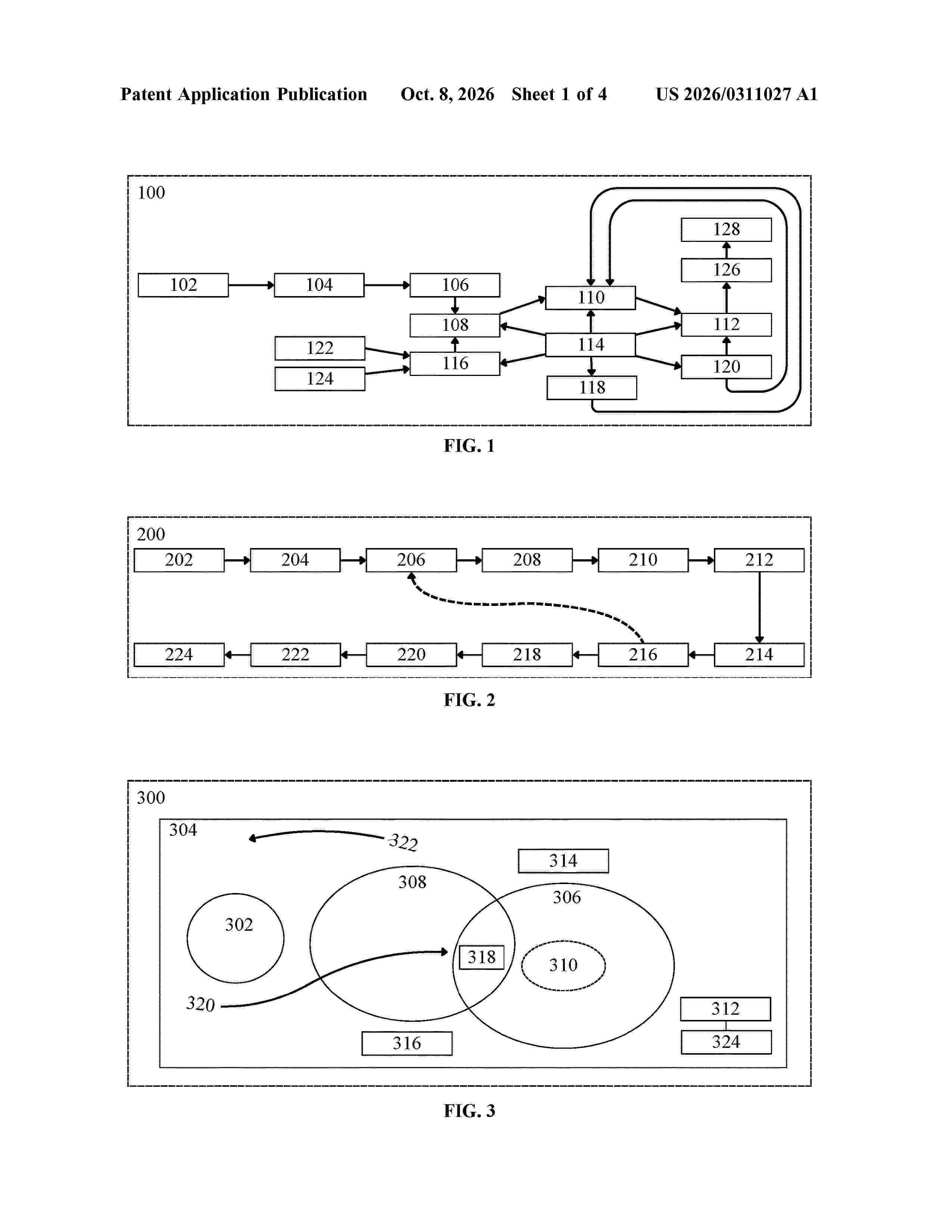
0000 A recognition-enhanced quantum search system, method, and computer-readable medium are disclosed in which a quantum search process distinguishes among marked solution states, a first class of non-solution states, and a second class of non-solution states during iterative amplitude amplification. A quantum state is prepared over a search domain, an oracle operation marks one or more candidate states satisfying a target criterion, a vantage metric is determined for at least a subset of non-solution states, a recognition diffusion operation is applied relative to a recognition-weighted state representation derived from the vantage metric, and a state-dependent transform applies different phase treatments to the different state classes. In representative embodiments, stronger suppression is applied to vantage-likely non-solution states than to other non-solution states. The process may use an effective-domain value for iteration control and may attenuate or bypass the state-dependent transform when the vantage metric is unavailable or insufficiently informative.
Resumen de: WO2026213127A1
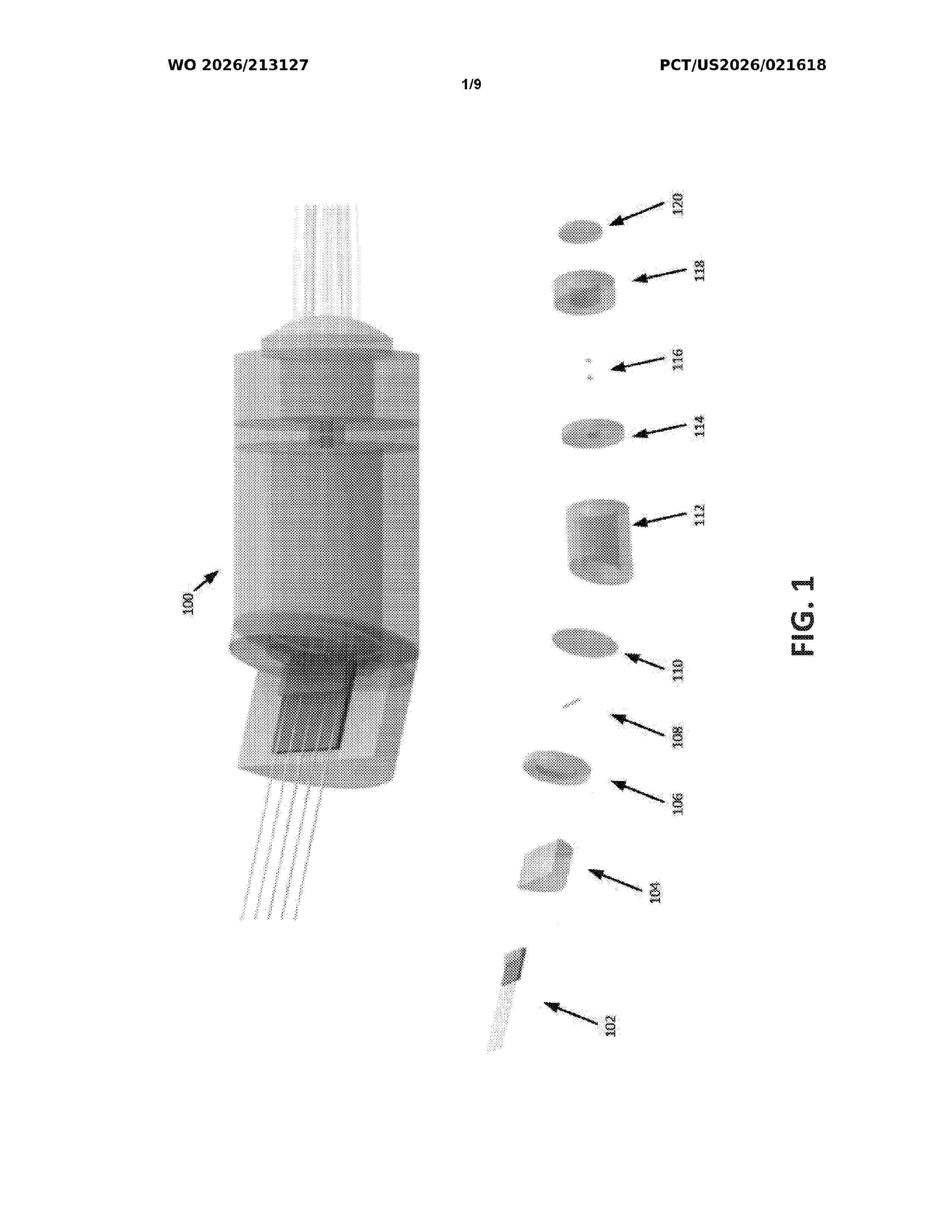
Example embodiments provide methods, systems, apparatuses, computer program products and/or the like for composite optical benches. A composite optical bench may comprise: one or more beam array sources hosted by a first housing; one or more beam-specific optics hosted by one or more second housings; and one or more optional global optics hosted by one or more third housings, wherein the first housing, the one or more second housings, and the one or more third housings are aligned using: an axial alignment configuration defining axial separation of elements hosted by the first housing, the one or more second housings, and the one or more third housings; and a radial alignment configuration wherein the one or more second housings and the one or more third housings are positioned after the first housing, and wherein the one or more second housings and the one or more third housings are variously positioned.
Nº publicación: US20260311025A1 08/10/2026
Solicitante:
DELL PRODUCTS L P [US]
Dell Products L.P.
Resumen de: US20260311025A1
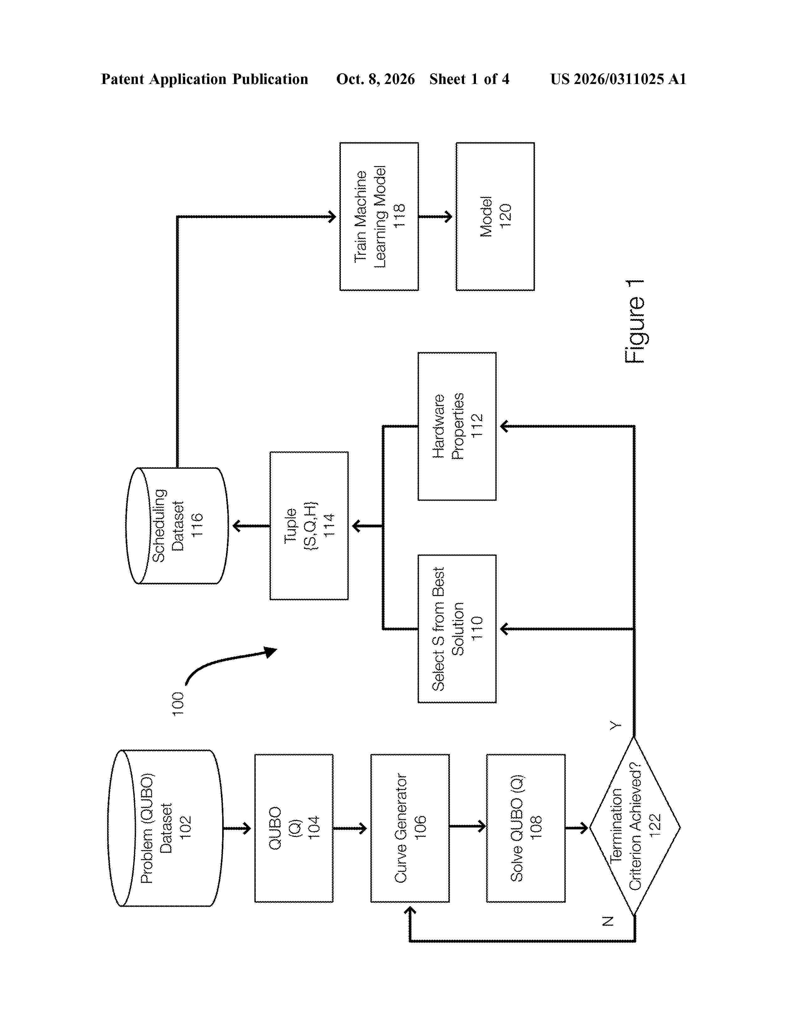
Selecting annealing schedules is disclosed. In a training phase, a model is trained using a scheduling dataset storing tuples of an annealing schedule, a problem, hardware properties. The tuples are generated by iteratively solving problems from a problem dataset using different annealing schedules. After reaching a termination criterion, the best annealing schedule is included in a tuple for the problem and stored in the scheduling dataset. In an inference phase, a problem is decomposed into subproblems that are then clustered. The model is used to select or infer an annealing schedule for representative subproblems selected from each of the clusters. The inferred annealing schedules assigned to the representative subproblems are used for the subproblems in the corresponding clusters. The subproblems are solved in quantum annealers and merged to determine a solution to the original problem.
 BOPI
BOPI
 Sede Electrónica