Si deseas distinguir tus productos, servicios o ambos de los de otra empresa, es posible que necesites una marca o nombre comercial. Descubre qué son, en qué consiste su procedimiento de registro y qué implica.

Información sobre los plazos de presentación de solicitudes de transformación de marcas de la Unión Europea en marca nacional española. Más información


Si tienes un nuevo dispositivo, producto o procedimiento que resuelva un problema técnico o tenga una ventaja práctica, existen distintas formas de protegerlo en España y en otros países. Descubre cómo hacerlo.

¿Tu innovación reside en la estética, la ornamentación o la apariencia de tu producto? Protégela mediante un diseño industrial. Descubre qué derechos confiere el registro y cómo realizar la tramitación.

Las indicaciones geográficas protegen el nombre de un producto originario de una zona geográfica, a la cual le debe una determinada calidad, reputación u otra característica. Descubre qué son, en qué consiste su procedimiento de registro y qué beneficios conceden.

Las patentes publicadas en todo el mundo son una valiosa fuente de información científica, técnica y comercial.

Si eres emprendedor/a o una empresa y quieres potenciar y mejorar la rentabilidad de tu negocio protegiendo de forma adecuada los activos intangibles de tu organización, en este espacio encontrarás lo necesario.


 224
resultados
 Última actualización
23/10/2026 [09:45:00]


 Resultados 175 a 200 de 224

Resumen de: CN122886833A
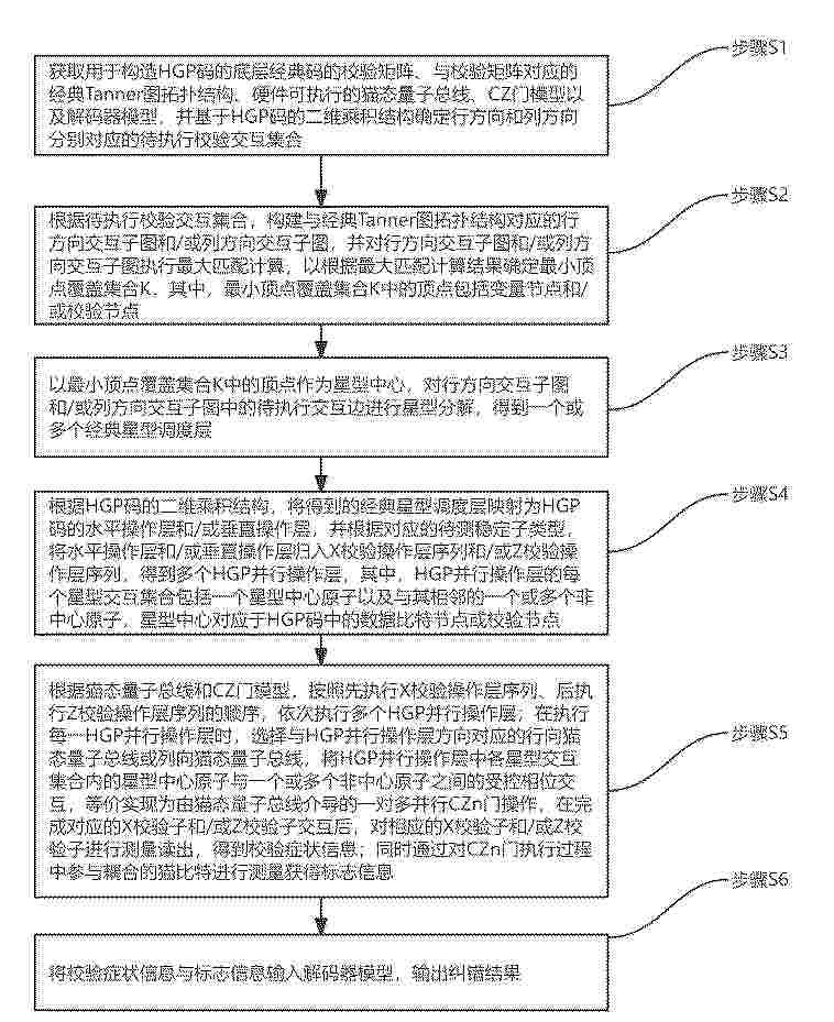
本发明涉及量子信息处理技术领域,提供一种基于猫态量子总线的HGP码症状提取与解码方法,包括确定待执行校验交互集合;构建对应的行方向交互子图和/或列方向交互子图,执行最大匹配计算确定最小顶点覆盖集合K;以顶点作为星型中心进行星型分解得到经典星型调度层;映射为HGP码的水平操作层和/或垂直操作层得到多个HGP并行操作层;依次执行多个HGP并行操作层;将校验症状信息与标志信息输入解码器模型输出纠错结果。通过星型分解调度与猫态量子总线介导的一对多并行门操作,实现HGP码非局域校验交互的高效症状提取,并利用猫比特测量结果作为标志信息辅助解码,提高纠错周期执行效率及线路级相关错误的区分能力。

Resumen de: WO2025149519A1
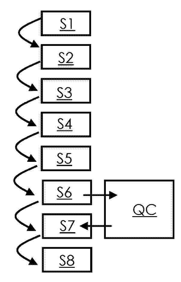
The described method is a method for determining an operations schedule that attributes each individual operation of two or more jobs to two or more machines, wherein the operations schedule is subject to an optimization towards an optimum of a key performance indicator indicating the performance of the operations schedule, wherein an operations schedule is initially encoded (S1, S2, S3, S4, S5) into a quantum register of a quantum computer (QC) and the optimization is performed (S6) using a variational quantum algorithm on the quantum computer (QC) acting on the quantum register and wherein an optimized operations schedule is provided (S7) by the quantum computer (QC).
Resumen de: US20260311907A1
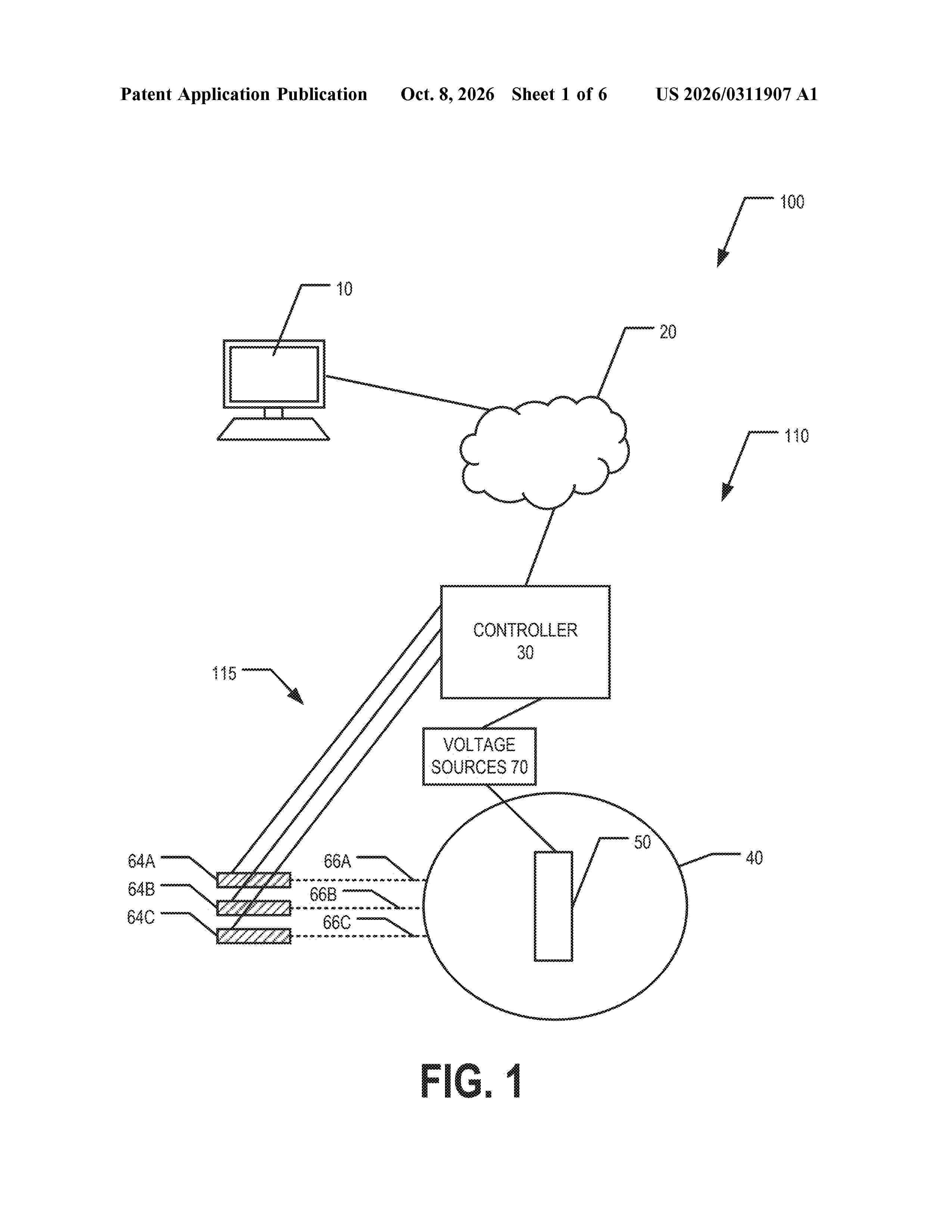
A confinement assembly is provided that includes an electrode layer comprising a plurality of electrodes, one or more routing layers configured to provide respective voltage signals to respective electrodes; and a ground plane comprising a set of features in electrical communication with one another and a load ground point connection. The electrodes include at least one radio frequency (RF) electrode and are operable to generate a confinement potential configured to confinement atomic objects. The respective voltage signals provided via the routing layers include an RF voltage signal configured to be provided to the RF electrode. The set of features is in electrical communication with the RF electrode and configured to guide a return RF current to ground along an at least partially constrained path. The return RF current is generated responsive to the RF voltage signal being provided to the RF electrode.
Resumen de: US20260311024A1
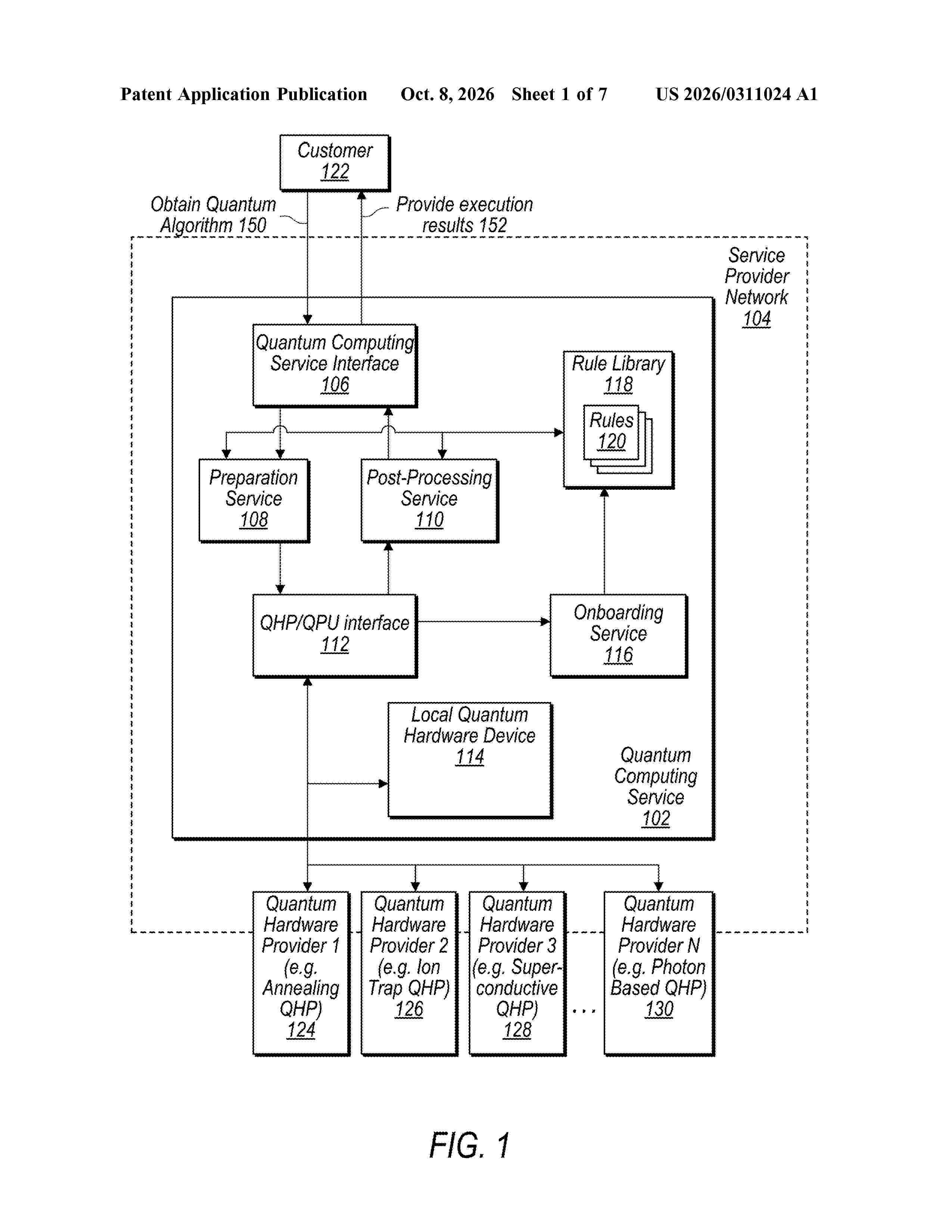
0000 Methods and apparatus for rule-based processing of quantum computing algorithms are described herein. Features of a quantum processing unit (QPU) may be onboarded to a quantum computing service provider using logical rules that, when executed, generate code used for preparing a quantum computing algorithm for execution on the QPU. For example, using the logical rules may decouple the functionalities of the quantum computing service from the features of QPU device capabilities.
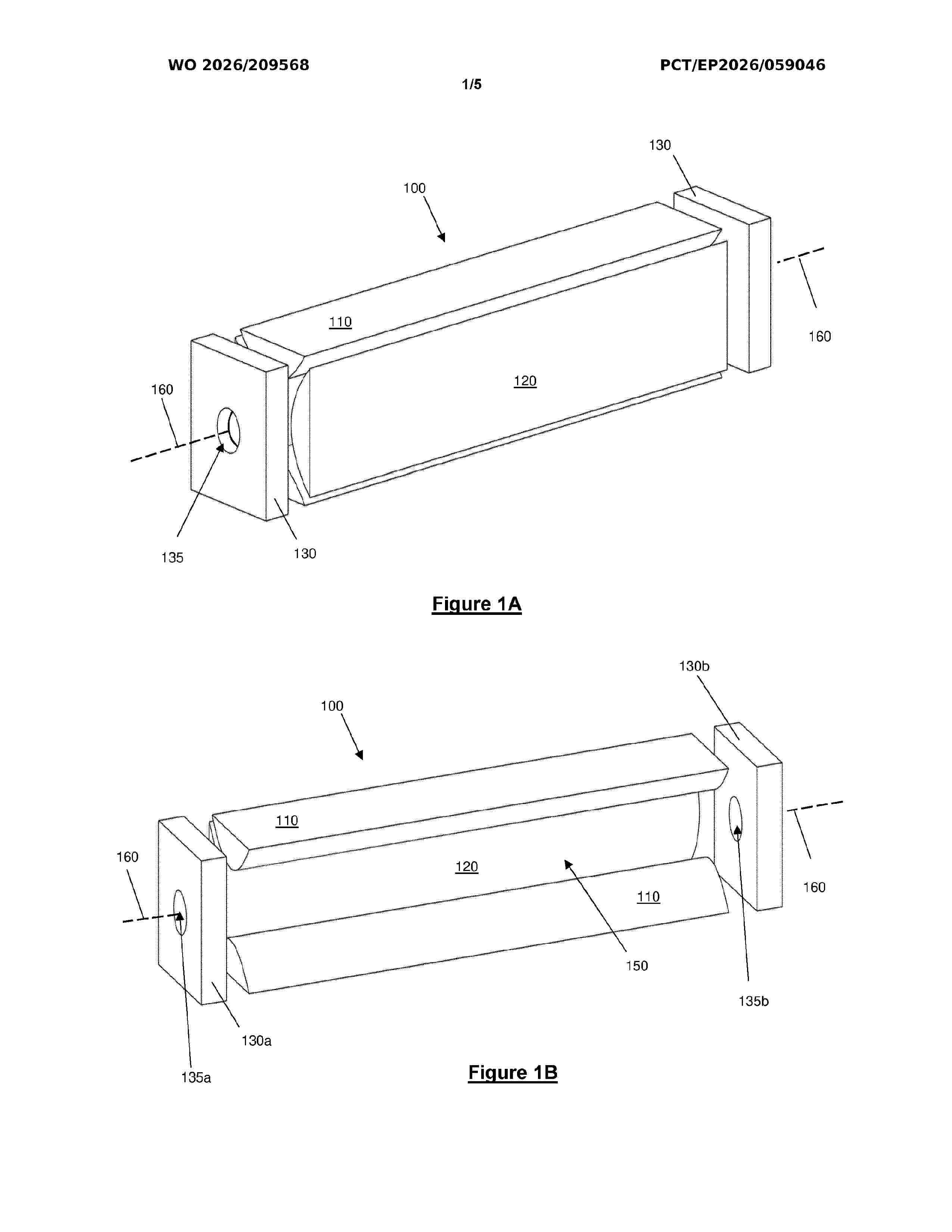
Resumen de: WO2026209568A1
A method of determining a location and velocity of one or more charged particles trapped within a charged particle trap by a trapping field is described. The charged particle trap comprises a trapping volume defined by trapping electrodes and a first pair of electrical conductors separated by at least a portion of the trapping volume along a first axis. The method comprises measuring an induced signal in each electrical conductor of the first pair of electrical conductors that is induced by the one or more charged particles' motion within the trapping volume. The measurements of the induced signals from the first pair of electrical conductors are used to determine a location of the one or more charged particles along the first axis and a velocity of the one or more particles along the first axis.
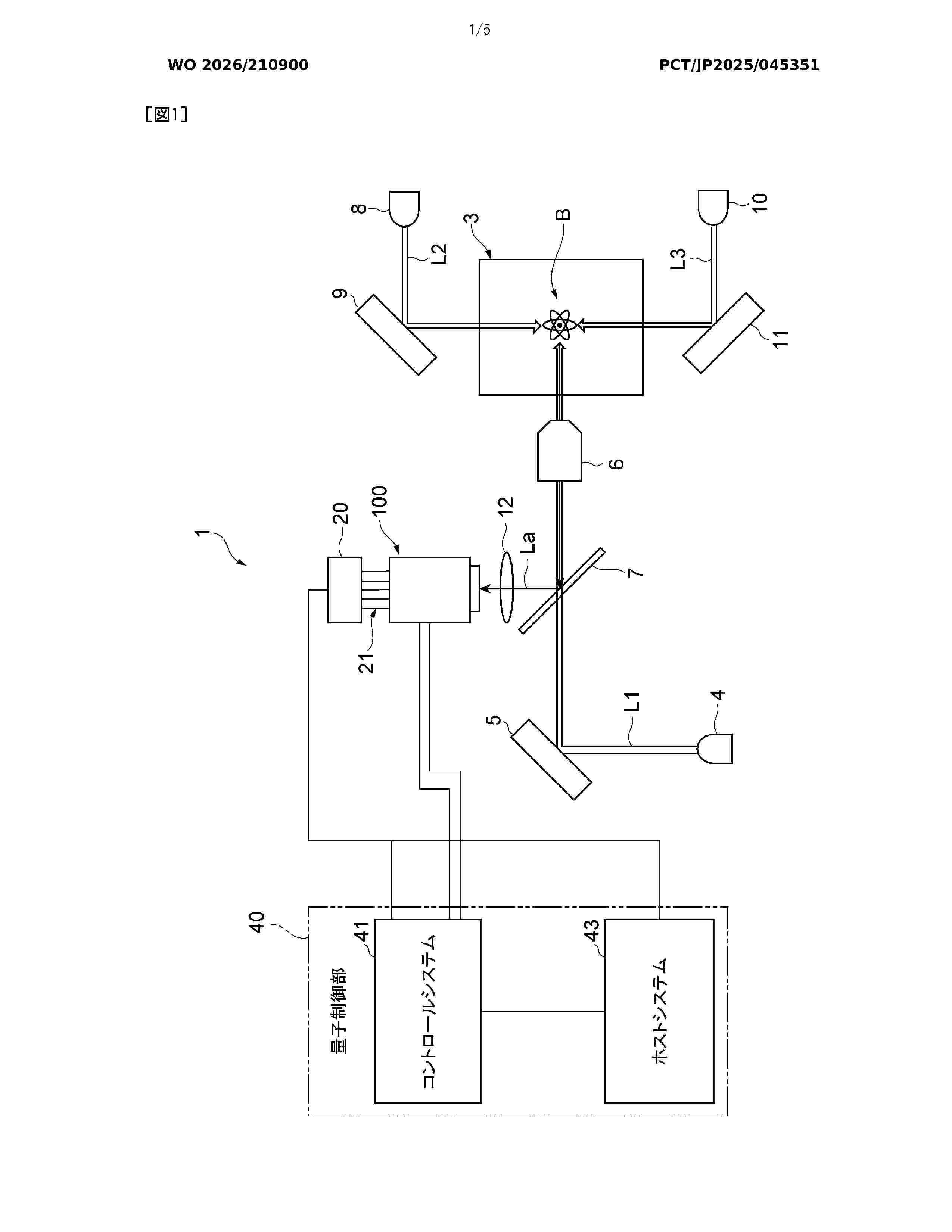
Resumen de: WO2026210900A1
A quantum bit detection module according to one aspect of the present invention comprises an image sensor and a sensor control unit. The image sensor is configured to be capable of presetting a first region and a second region, which are mutually different, as exposure regions in an imaging region. The sensor control unit has a first trigger input terminal, to which a first trigger signal is input, and a second trigger input terminal, to which a second trigger signal different from the first trigger signal is input. The image sensor performs imaging while switching between the first region and the second region in response to the first trigger signal and the second trigger signal.
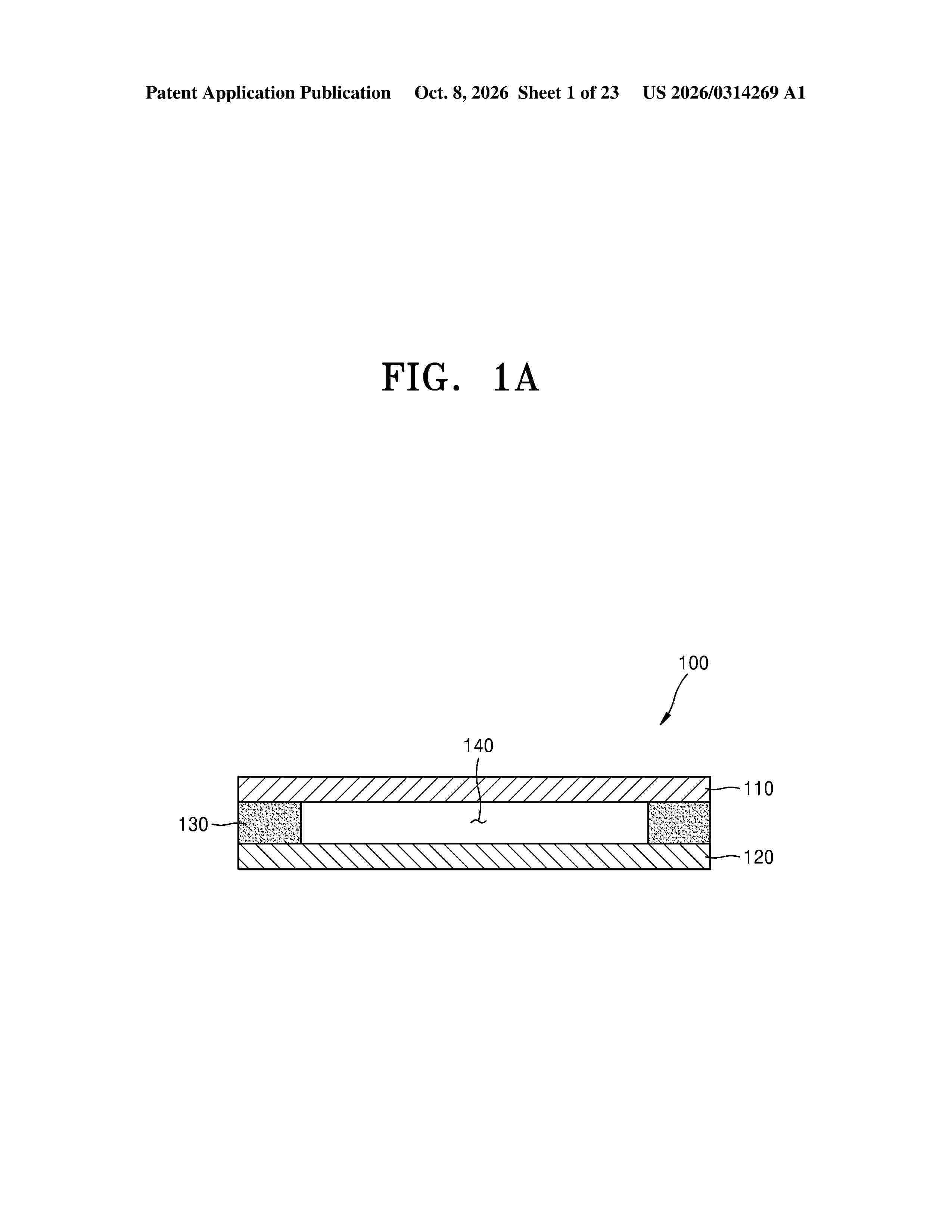
Resumen de: US20260314269A1
A superconducting quantum chip including a first chip including a superconducting quantum device having a controllable resonant frequency, a second chip bonded to the first chip with a gap defined between the first chip and the second chip, and a ferromagnetic device provided on the second chip, the ferromagnetic device being configured to apply a magnetic field to the superconducting quantum device to control a resonant frequency of the superconducting quantum device.
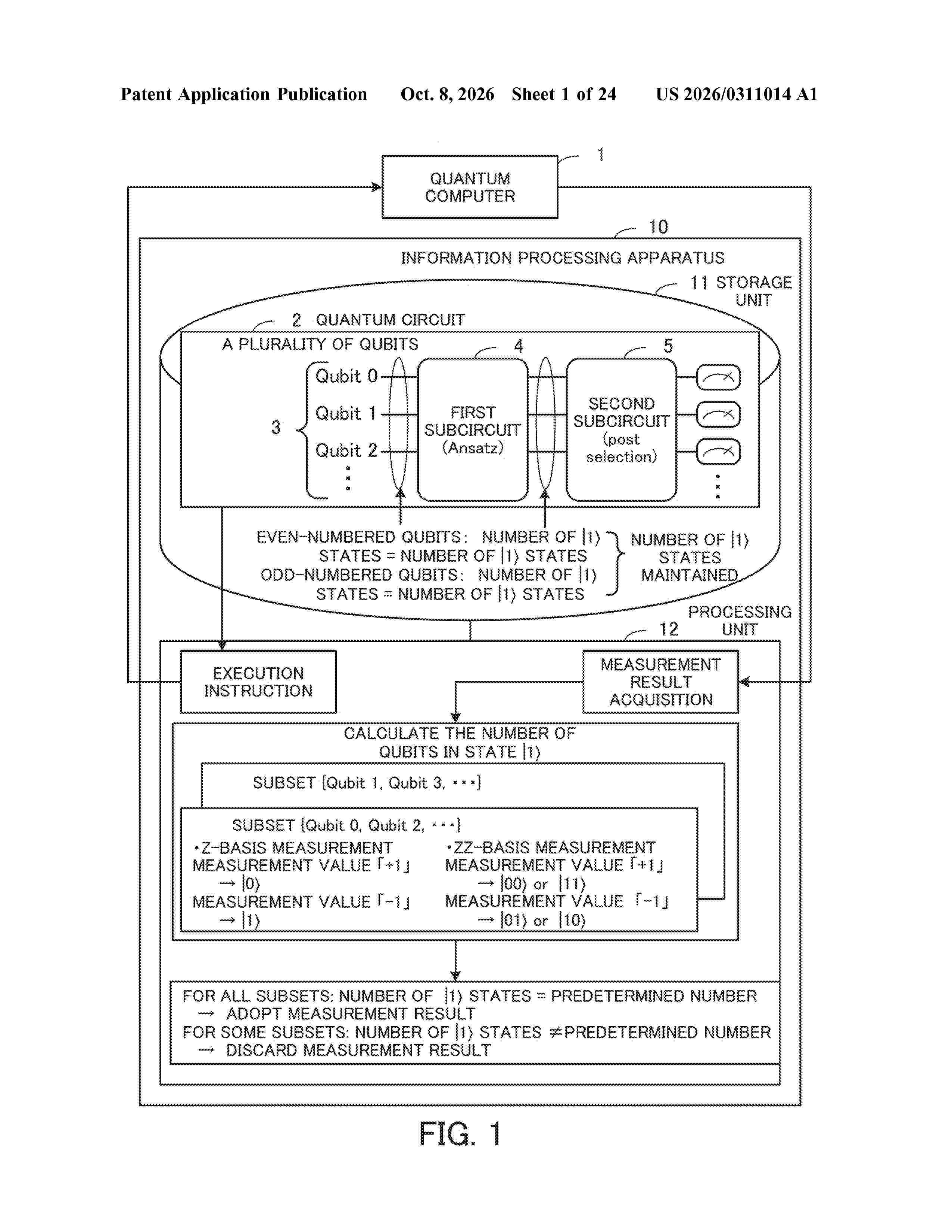
Resumen de: US20260311014A1
An information processing apparatus instructs a quantum computer to execute a quantum circuit in which, among first qubits having a predetermined attribute included in a plurality of qubits, a predetermined number of first qubits are in a state |1 before a gate operation specified by a first subcircuit. The information processing apparatus acquires, from the quantum computer, a measurement result indicating the state of each qubit after gate operations specified by the quantum circuit. The information processing apparatus calculates, based on the states of the first qubits indicated by the measurement result, the number of first qubits that are in the state |1 after the gate operation specified by the first subcircuit. Then, the information processing apparatus discards the measurement result, if the number of first qubits that are in the state |1 after the gate operation specified by the first subcircuit is different from the predetermined number.
Resumen de: WO2026207830A1
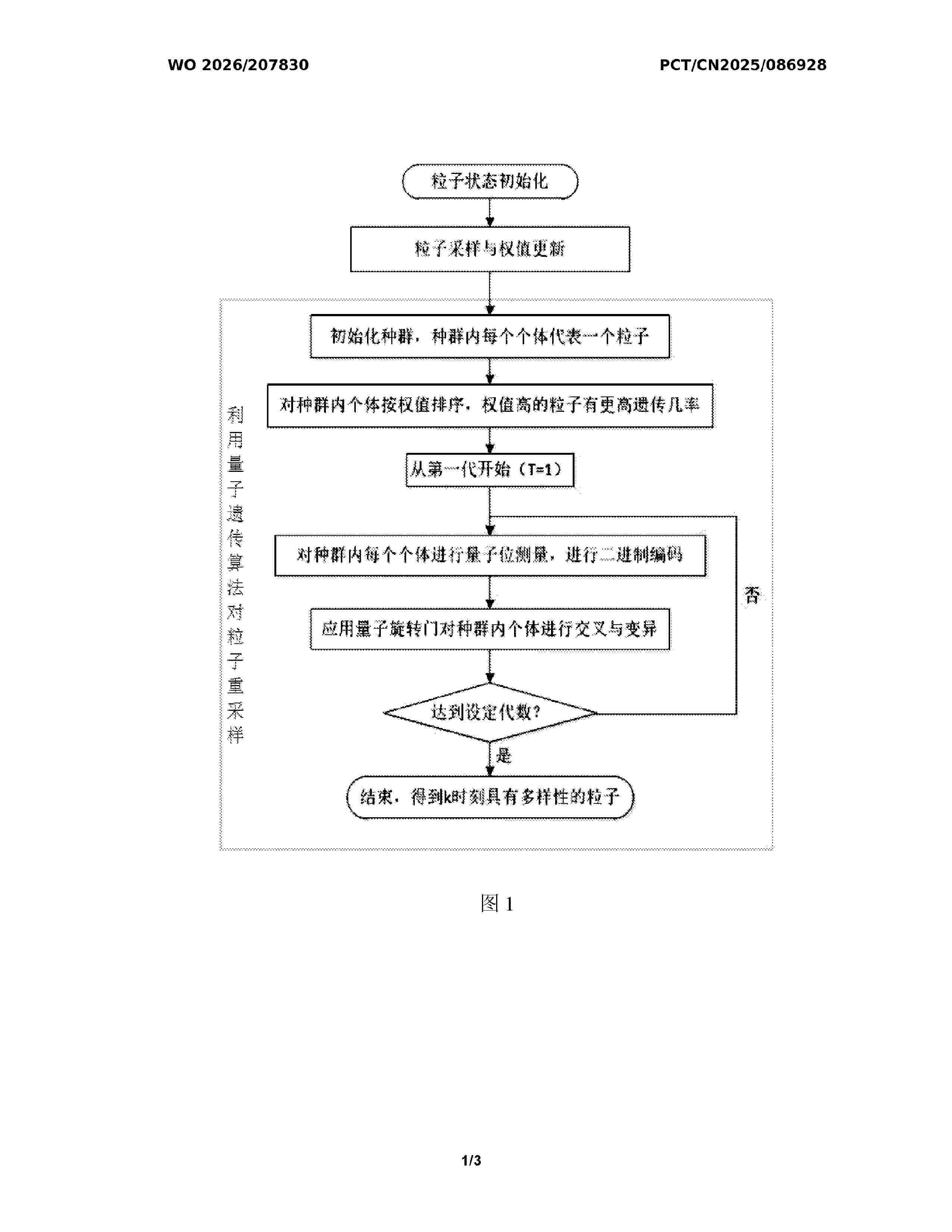
A mobile robot navigation and map construction system. A robot mainly uses visual information to estimate its own position and landmark positions by means of a particle filtering algorithm combined with a quantum genetic algorithm, generates a navigation map by means of the estimation of the landmark positions, and finally implements path exploration by means of a backtracking tree. During the path exploration process of the robot, a two-step filtering method is used to detect landmarks, identify landmarks, and gradually confirm landmark information so as to form a topological map.
Resumen de: US20260314275A1
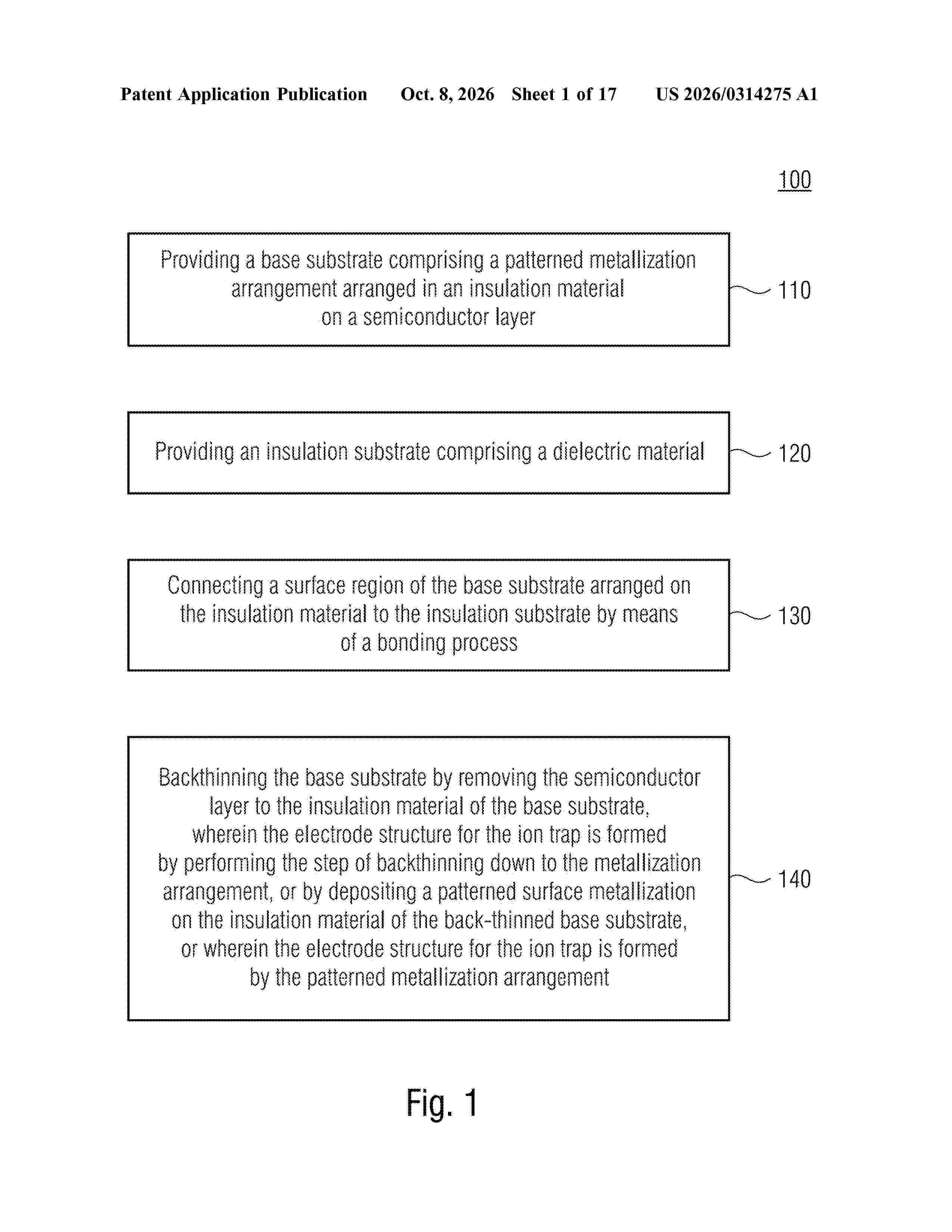
A method for manufacturing an electrode structure for an ion trap includes providing a base substrate comprising a patterned metallization arrangement arranged in an insulation material on a semiconductor layer, providing an insulation substrate comprising a dielectric material, connecting a surface region of the base substrate arranged on the insulation material to the insulation substrate by means of a bonding process, and backthinning the base substrate by removing the semiconductor layer to the insulation material of the base substrate, wherein the electrode structure for the ion trap is formed by performing the step of backthinning to the metallization arrangement or by depositing a patterned surface metallization on the insulation material of the back-thinned base substrate, or wherein the electrode structure for the ion trap is formed by the patterned metallization arrangement.
Resumen de: US20260311021A1
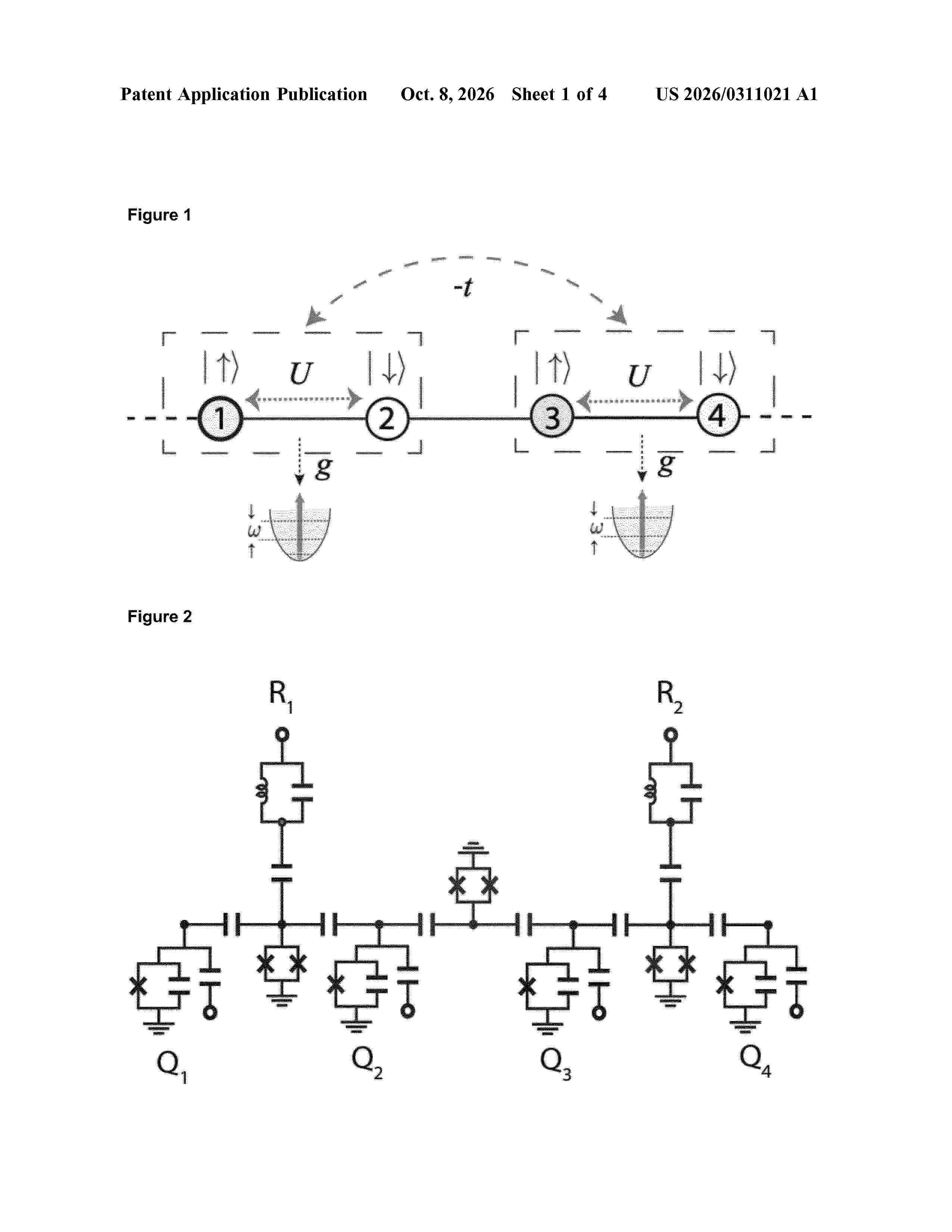
0000 The invention relates to a computer-implemented method, to a computer program, and to a computer device as described herein. In particular, the invention relates to a hybrid digital-analog method for simulating fermion-boson interactions using superconducting circuits, where the target Hamiltonian H comprises tunnelling interactions, Coulomb repulsion, and at least one electron and phonon term such as the Hubbard-Holstein model, Hubbard model, Holstein model, and/or Bose-Hubbard model.
Resumen de: WO2026212588A2
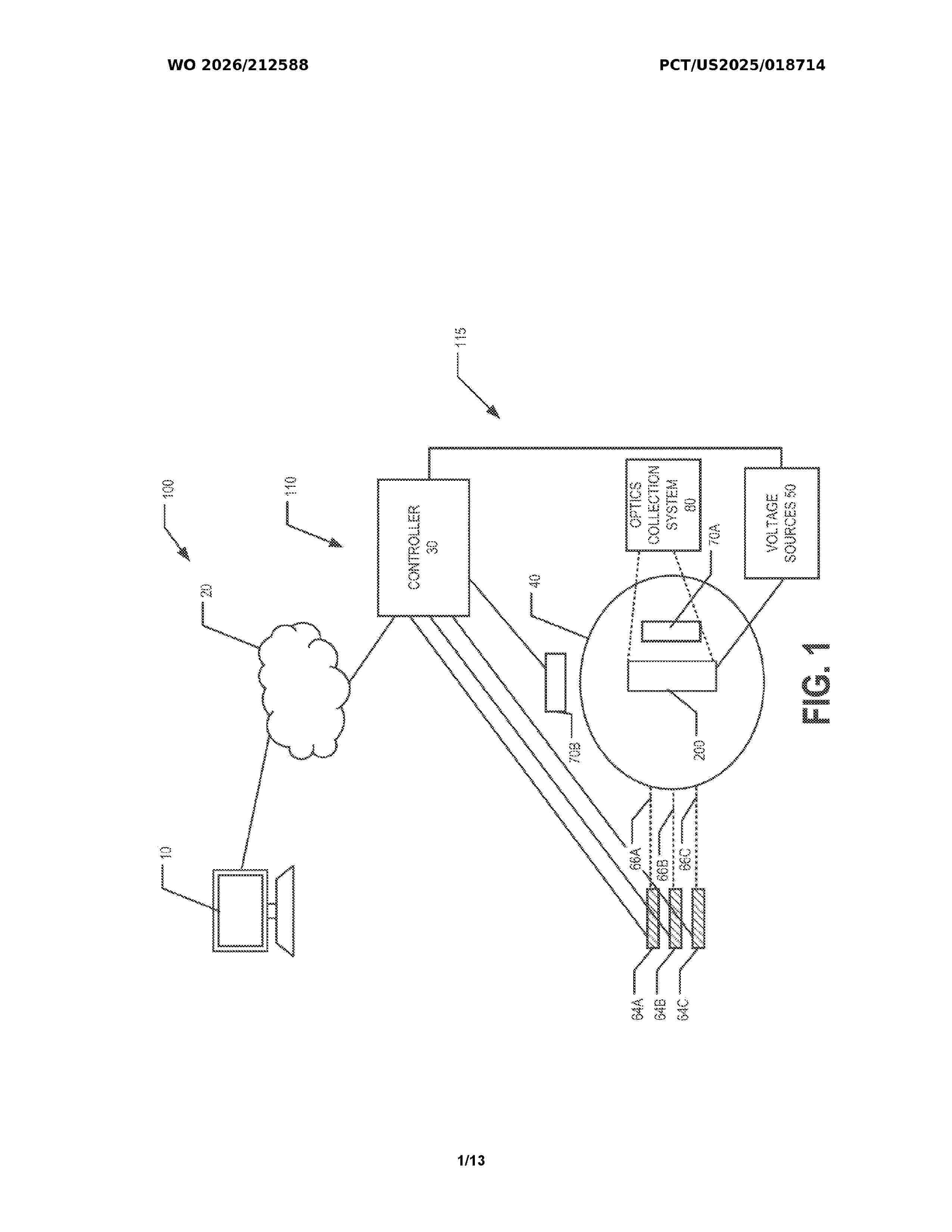
An atomic object confinement apparatus includes a substrate comprising a plurality of metal routing features; a plurality of electrodes disposed on a surface of the substrate and in electric communication with respective metal routing features of the plurality of metal routing features; and a plurality of gaps. Respective gaps of the plurality of gaps disposed between adjacent electrodes of the plurality of electrodes. Respective exposed surfaces of the plurality of electrodes have root mean square (RMS) roughness of 10 nm or less.
Resumen de: US20260311019A1
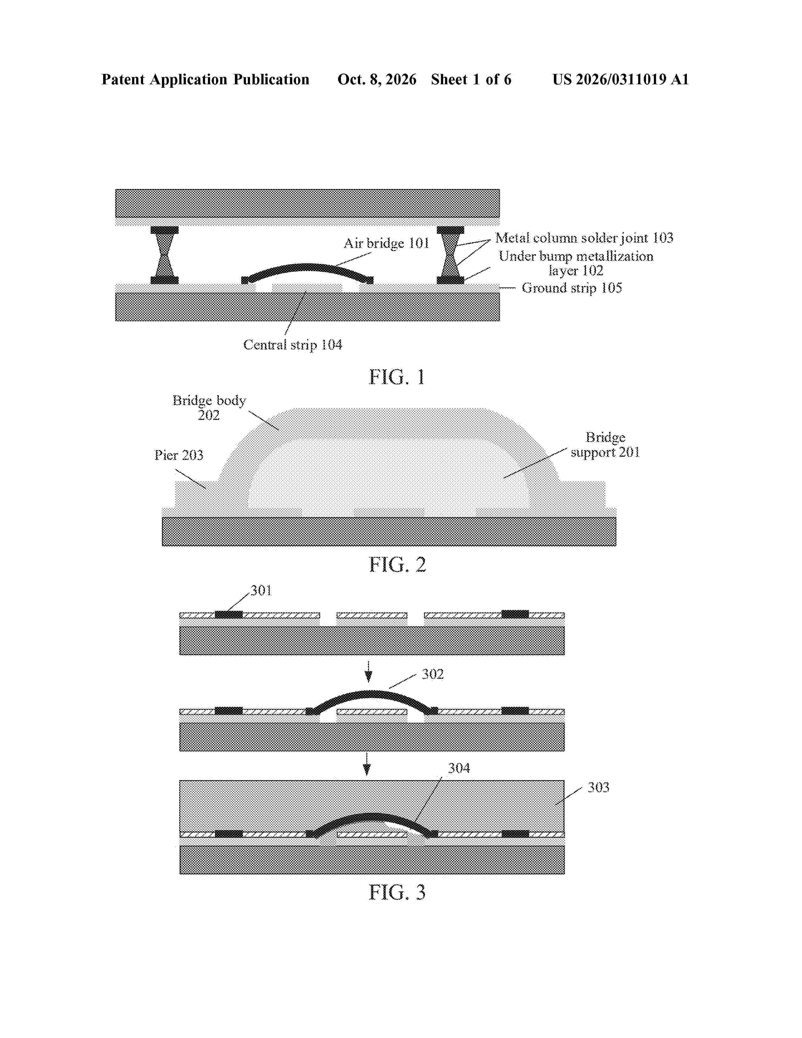
0000 This application discloses a method for preparing a quantum chip, a quantum chip, and a quantum computer, related to the technical field of quantum chips. The method includes: spin-coating a positive photoresist on a substrate, and preparing an under bump metallization (UBM) layer and an air bridge on the substrate spin-coated with the positive photoresist, to obtain a first substrate structure; spin-coating a negative photoresist on the first substrate structure, and preparing a metal column solder joint on the first substrate structure spin-coated with the negative photoresist, to obtain a second substrate structure; and removing the positive photoresist and the negative photoresist from the second substrate structure, to obtain a quantum chip including the UBM layer, the air bridge, and the metal column solder joint. By using the method provided in exemplary embodiments of this application, preparation efficiency can be improved, and performance of the chip can be improved.
Resumen de: US20260311031A1
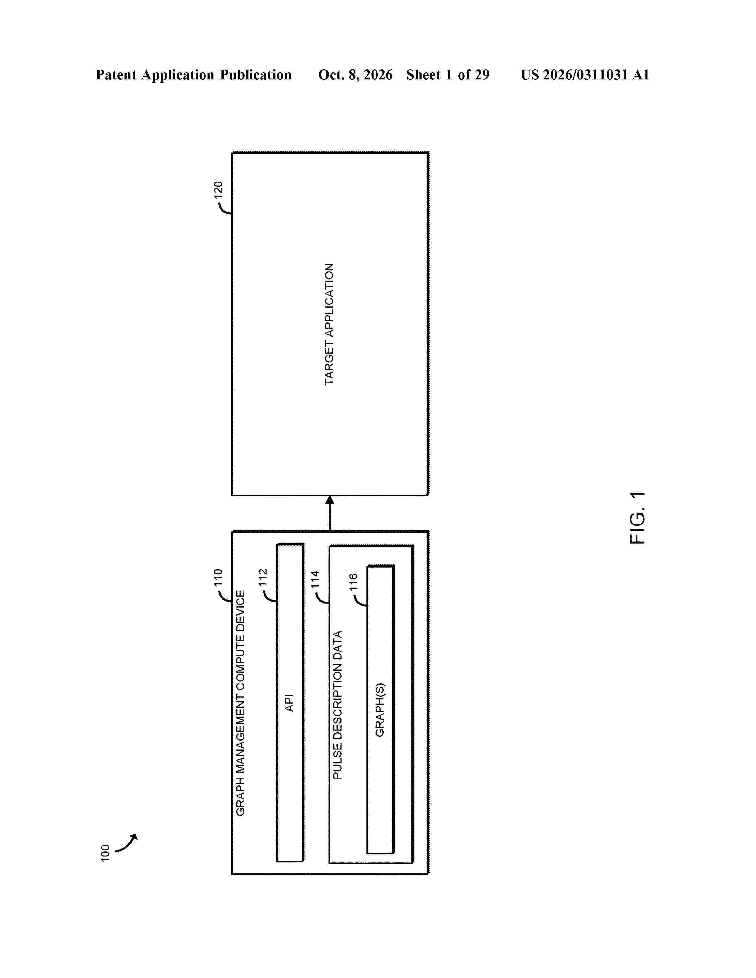
Technologies for providing pulse-level access in a quantum computing system based on a graph-based architecture include a compute device with circuitry configured to obtain pulse description data indicative of a graph representing one or more parameters of at least one waveform that defines at least one pulse. The circuitry may also be configured to perform analysis operations on the graph to determine properties of the at least one pulse and produce a corresponding target pulse description based on the analysis. The circuitry may be additionally configured to provide the target pulse description to a target application to produce the at least one pulse.
Resumen de: US20260313976A1
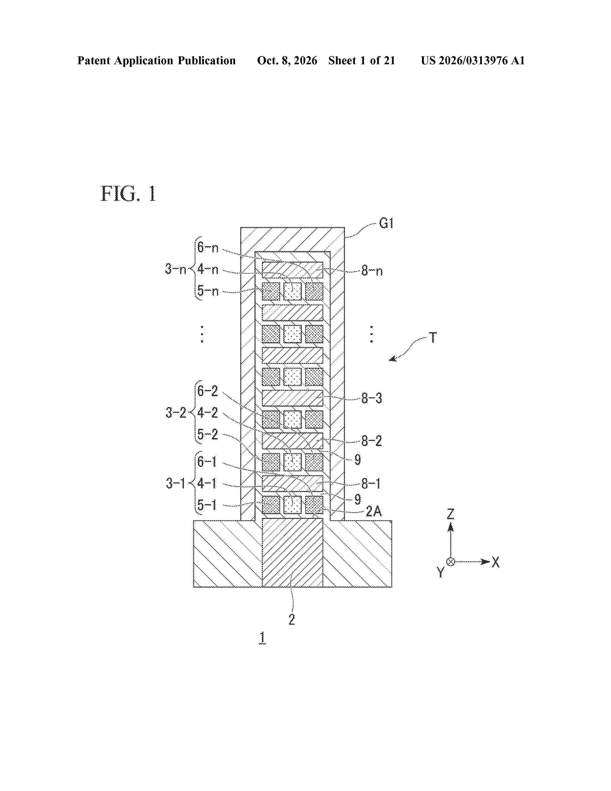
A semiconductor quantum device according to the present disclosure includes a transistor structure portion having a source, a drain, and a gate, one or more quantum dot structure portions capable of localizing charges; and a qubit control current line capable of changing states of the charges in the quantum dot structure portions, in which the quantum dot structure portions and the qubit control current line are disposed in the same layer, and the transistor structure portion and the quantum dot structure portions are laminated in a lamination direction with respect to a substrate.
Resumen de: US20260311023A1
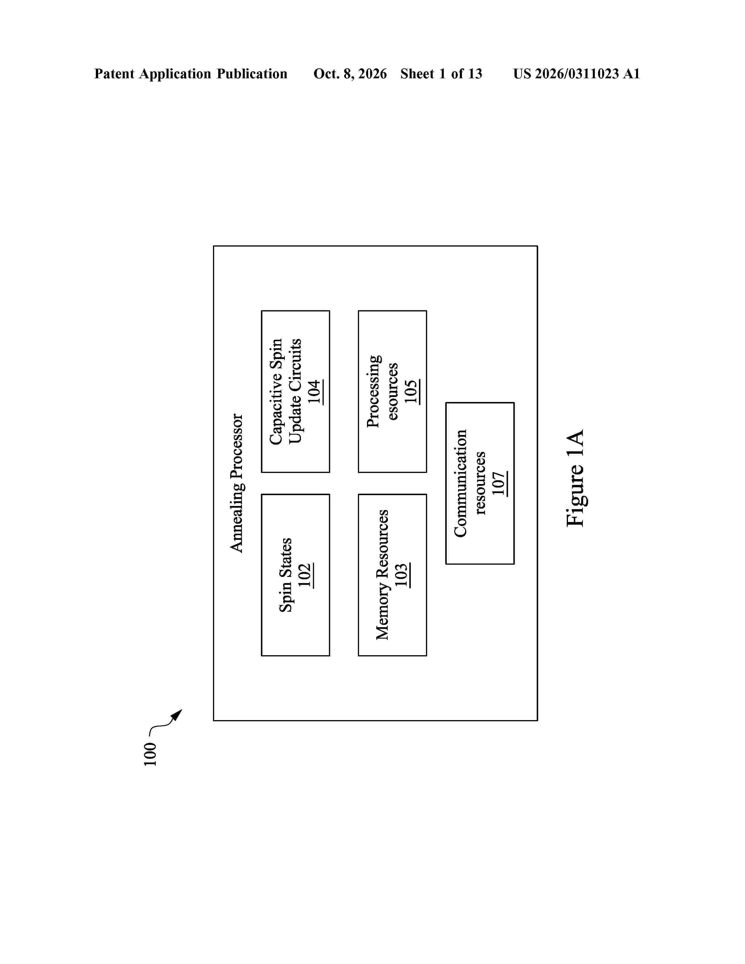
An annealing processor utilizes capacitive spin update circuits to generate values for determining if spin states should be updated. Each capacitive spin update circuit induces a voltage on a main capacitor via capacitive coupling with a plurality of capacitors of corresponding bit cells. Each bit cell receives a spin value and a spin coupling value. The induced charge is based, in part, on the spin values and spin coupling values.
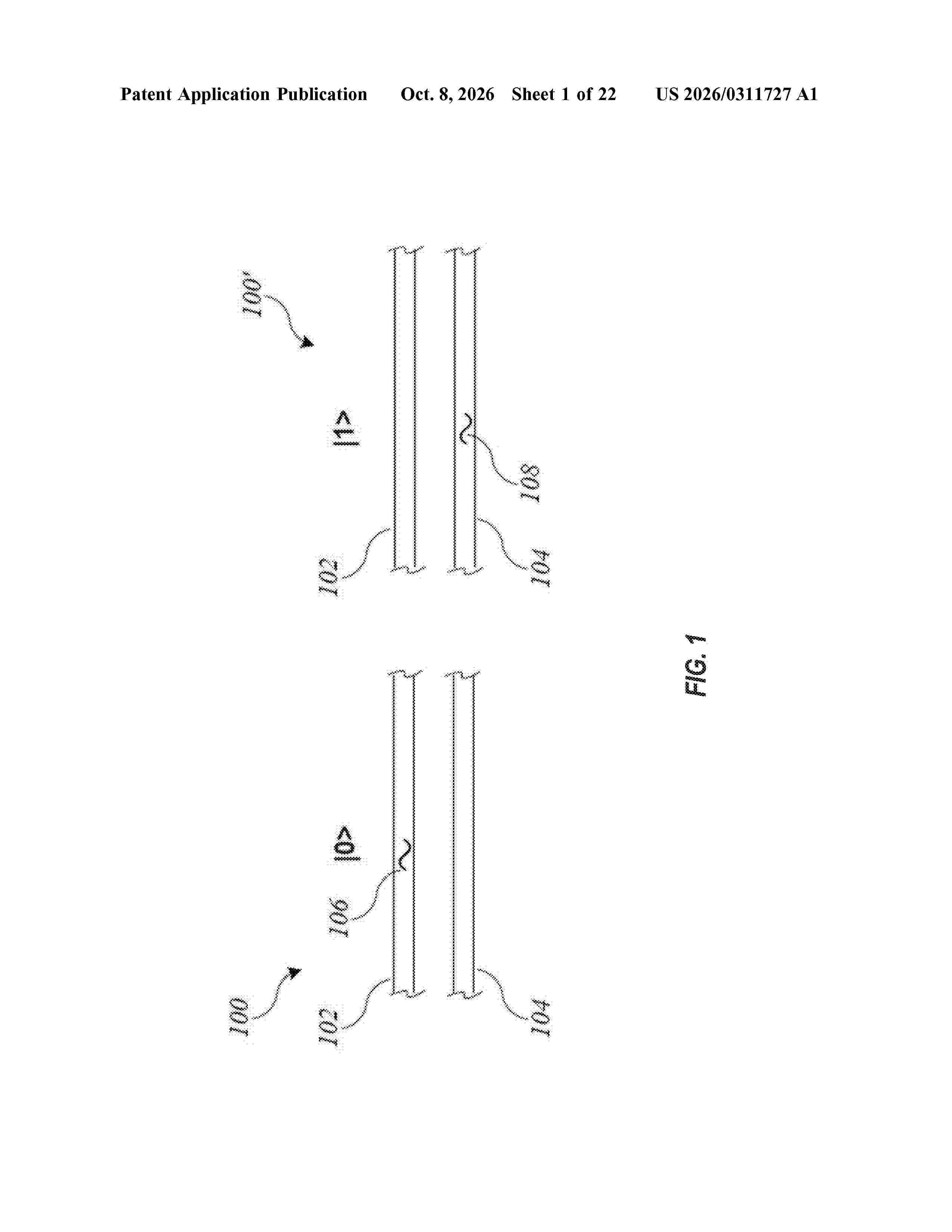
Resumen de: US20260311727A1
A system includes a first photonic integrated circuit. The circuit includes a qubit encoder configured to receive a spatial-mode qubit and convert the spatial-mode qubit to a temporal-mode qubit and an optical interconnect configured to receive and transmit the temporal-mode qubit. The system further includes a second photonic integrated circuit, itself including a qubit decoder configured to receive the temporal-mode qubit and convert the temporal-mode qubit back into the spatial-mode qubit.
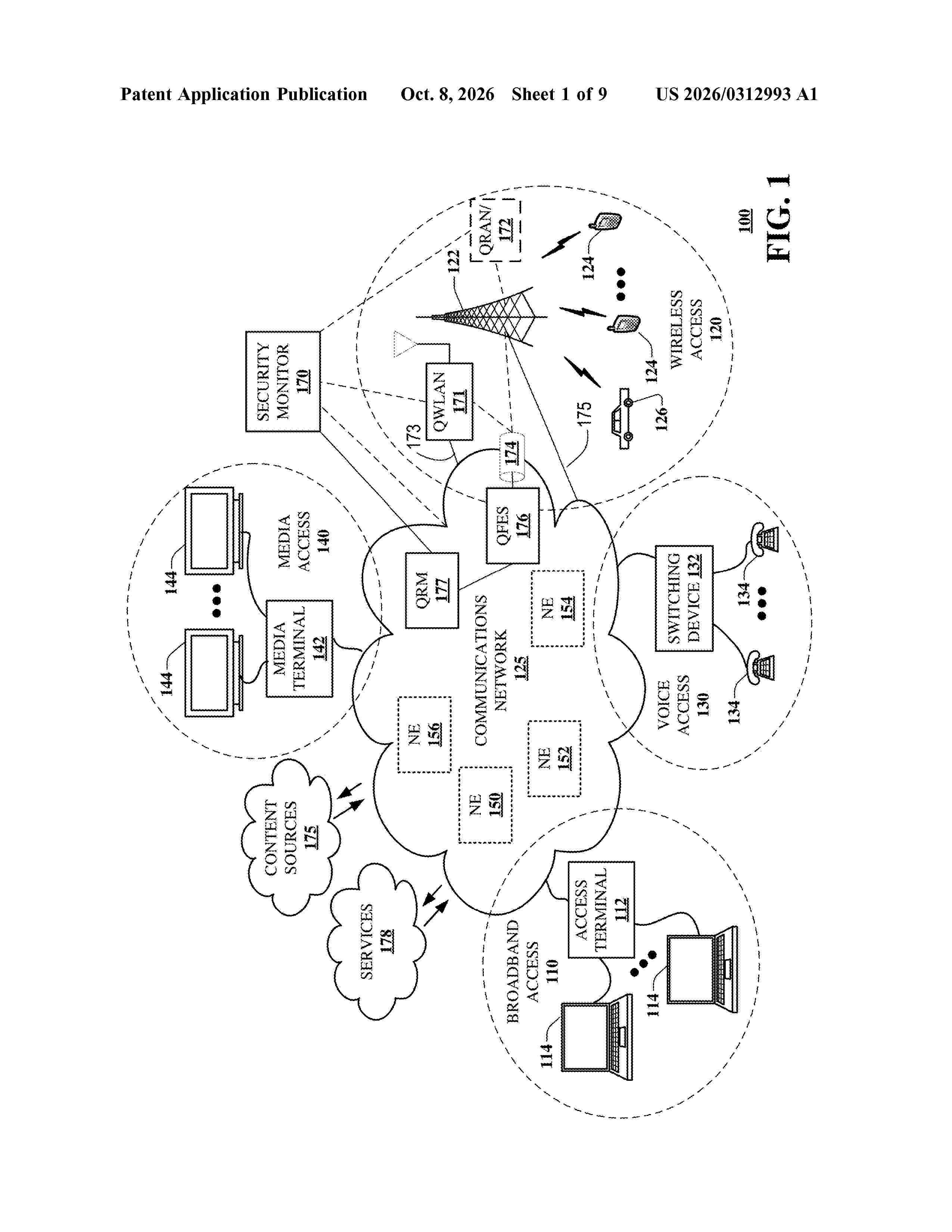
Resumen de: US20260312993A1
0000 Aspects of the subject disclosure may include, for example, monitoring a security status of a wireless communication session comprising a back-haul link supporting a classical communication channel between a wireless access point and a wireless mobility core network. The classical communication channel is adapted to transport underlying data of the wireless communication session and, responsive to determining a change in the security status, associating with the wireless communication session a quantum communication channel adapted to transport information via qubits. Information is exchanged between the wireless access point and the mobility core network via the qubits of the quantum communication channel, wherein the exchanging of the information via the qubits enhances a security level of the wireless communication session in view of a perceived threat. Other embodiments are disclosed.
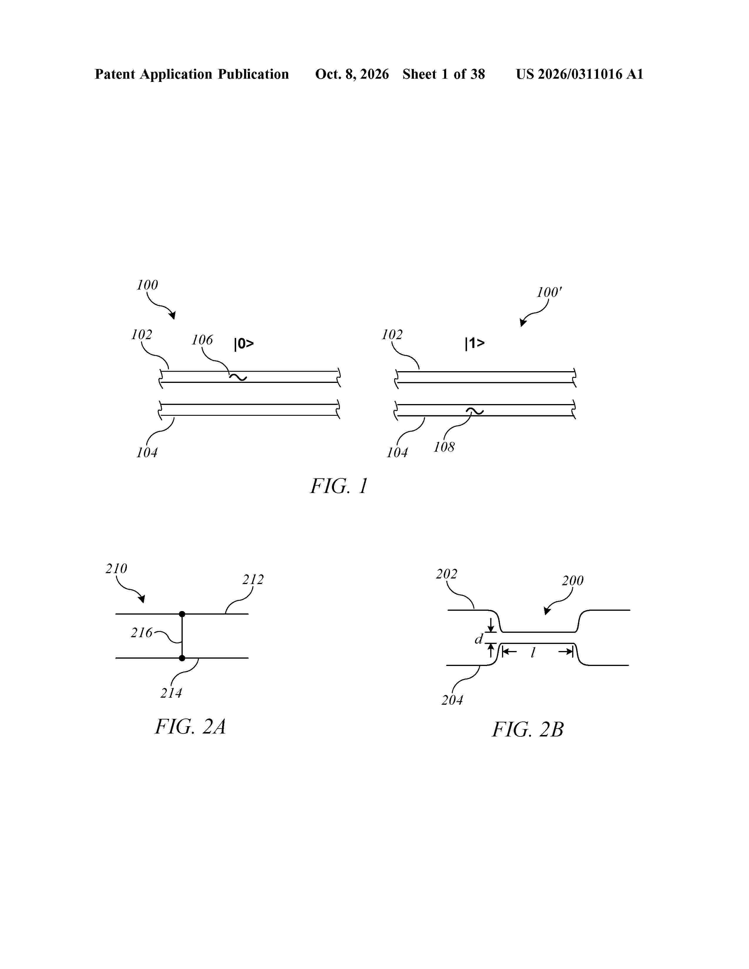
Resumen de: US20260311016A1
Entanglement among qubits can be generated using “rasterized” and interleaving techniques. A circuit can include a resource state generator that generates one resource state per clock cycle, with each resource state having a number of entangled qubits. The circuit can also include circuits and delay lines to perform entangling measurement operations on qubits of resource states generated by the same resource state generator in different clock cycles. With appropriate selection of delay lines, a single resource state generator can generate all of the resource states needed to generate a large entanglement structure. Hybrid techniques can also be used, where the number of resource state circuits is greater than one but less than the number of resource states needed to generate the entanglement structure.
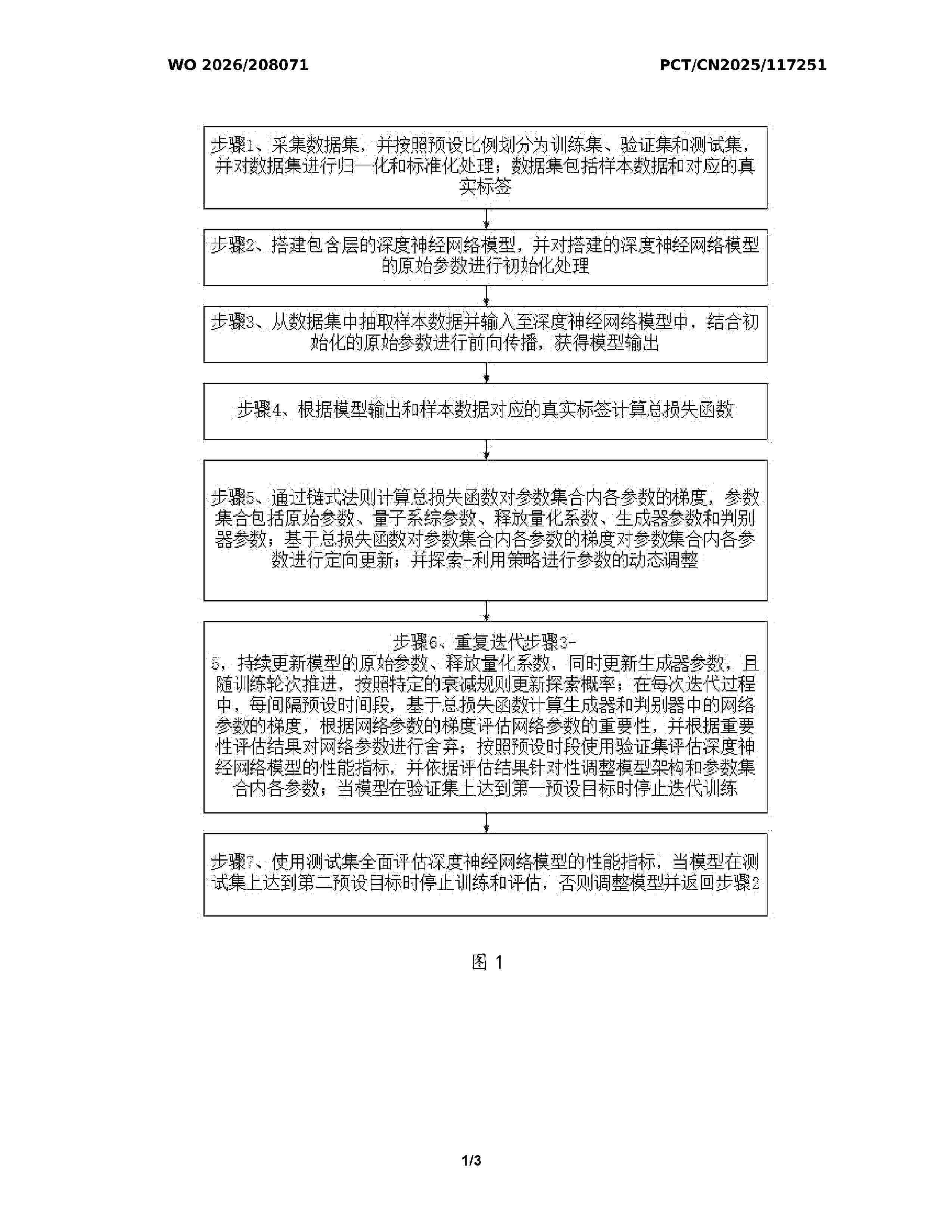
Resumen de: WO2026208071A1
The present invention relates to the technical field of artificial intelligence, and disclosed are an efficient neural network model compression system and method based on differentiable quantization with relaxation. The method comprises: step 1: collecting a dataset, and dividing the dataset into a training set, a validation set, and a test set; step 2: constructing a neural network model containing L layers and performing initialization processing; step 3: extracting sample data from the dataset, inputting the sample data into the neural network model for forward propagation, and obtaining a model output; step 4: calculating a total loss function; step 5: calculating gradients of the total loss function with respect to parameters, performing directed updating on the parameters, and dynamically adjusting the parameters by means of an exploration-exploitation strategy; step 6: iteratively repeating steps 3 to 5, and stopping iterative training when a first preset target is achieved; and step 7: evaluating performance indicators of the neural network model until a second preset target is achieved, and then stopping training and evaluation. The present invention achieves more efficient compression while maintaining model accuracy.
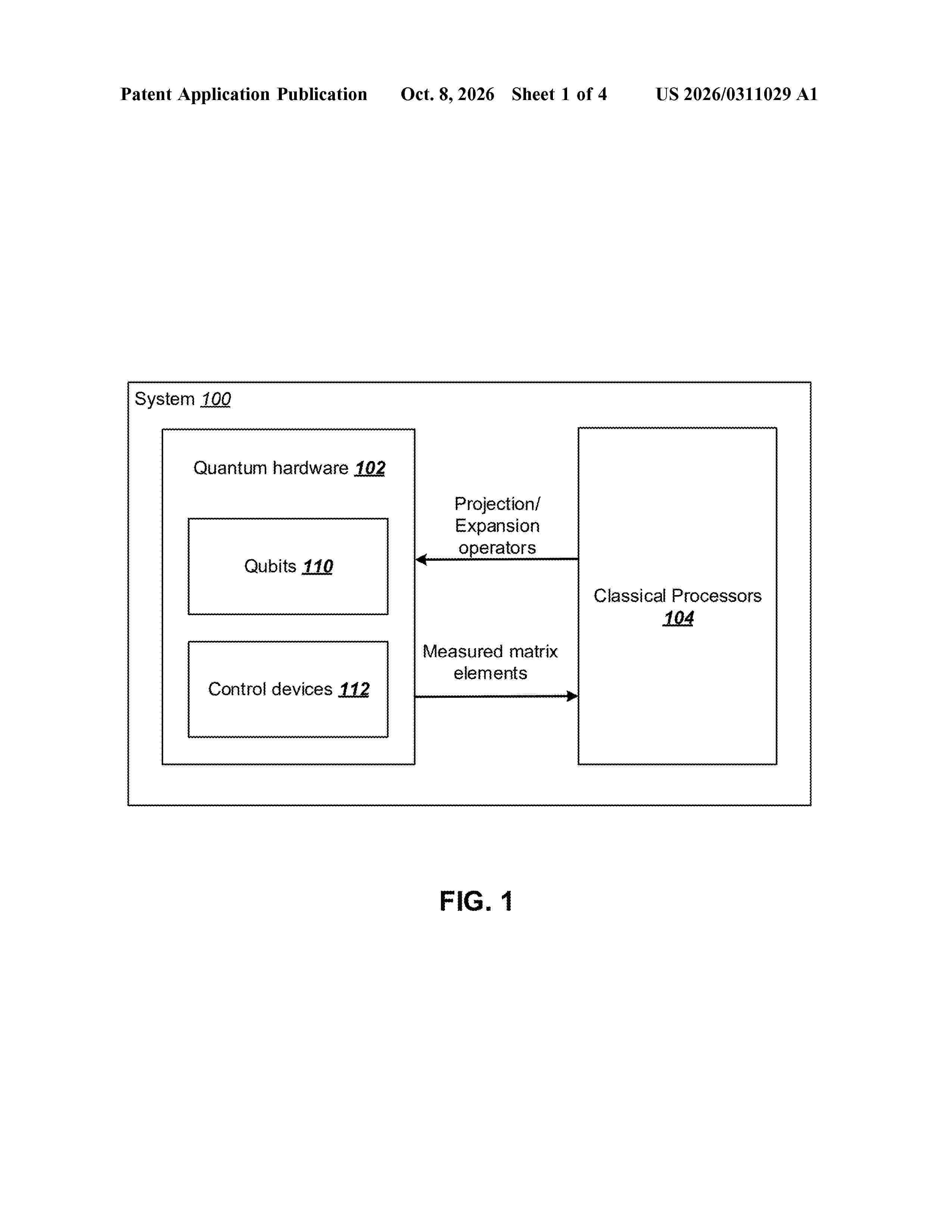
Resumen de: US20260311029A1
Methods, systems and apparatus for correcting a result of a quantum computation. In one aspect, a method includes selecting a quantum error correcting code for the quantum computation, wherein the quantum error correcting code is defined by multiple stabilizer generators; determining a set of symmetry operators, comprising: selecting a subset of the stabilizer generators, determining, for each selected stabilizer generator, a sum between an identity operator and the stabilizer generator, and multiplying the determined sums together to form a summation of terms, wherein each term in the summation is equal to a respective symmetry operator; measuring a projective correction of a physical observable over an output quantum state of the quantum computation using the determined set of symmetry operators, wherein the physical observable corresponds to the result of the quantum computation; and determining a corrected result of the quantum computation using the measured projective correction of the physical observable.
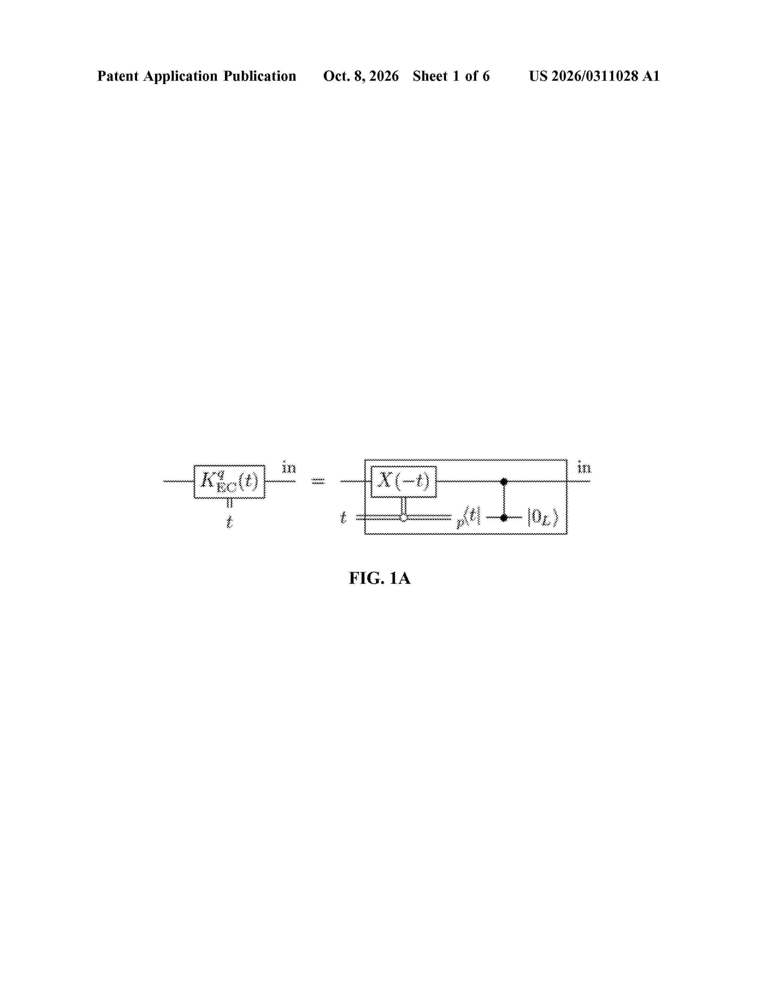
Resumen de: US20260311028A1
Applying Gottesman-Kitaev-Preskill (GKP) error correction to Gaussian input states, such as vacuum, produces distillable magic states, achieving universality without additional non-Gaussian elements. Gaussian operations are sufficient for fault-tolerant, universal quantum computing given a supply of GKP-encoded Pauli eigenstates.
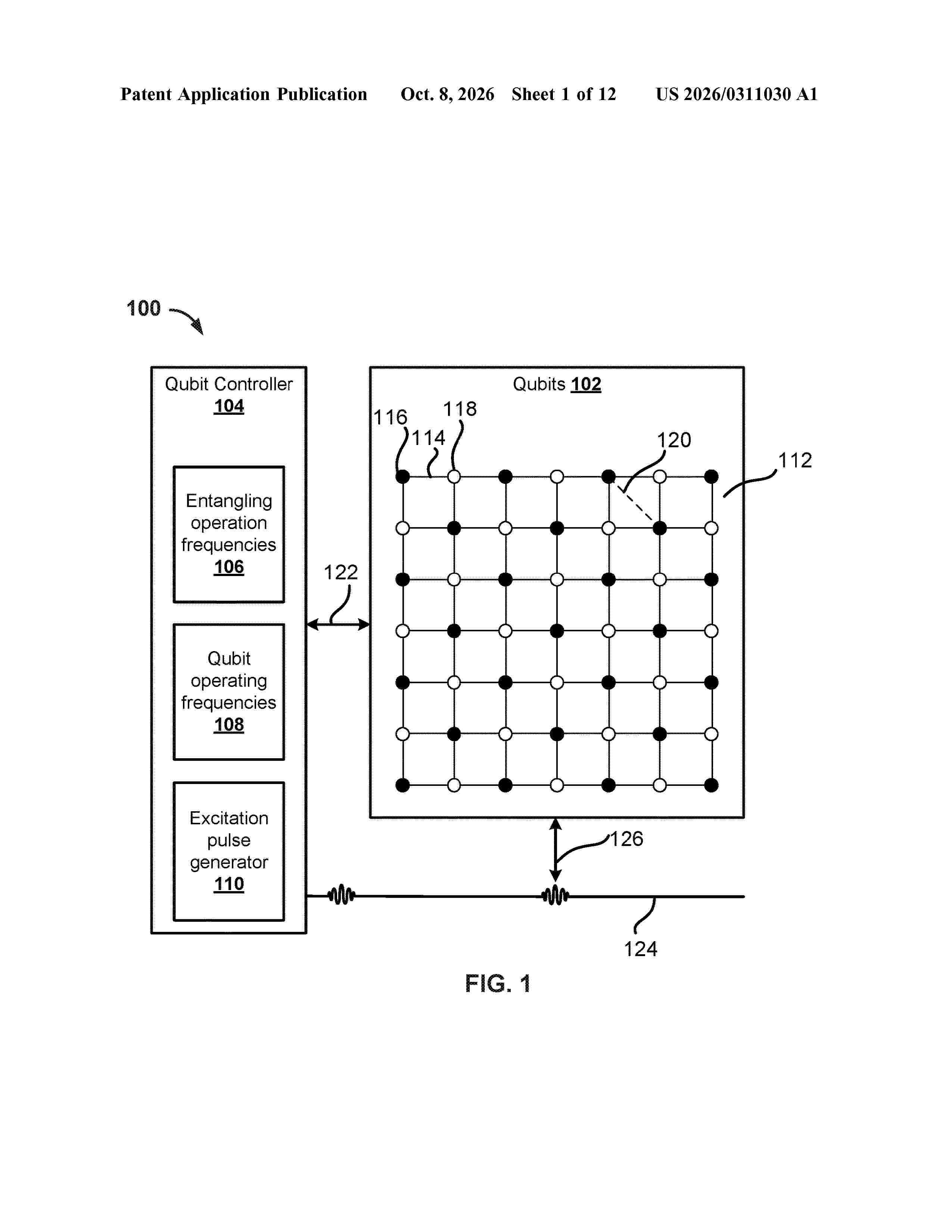
Resumen de: US20260311030A1
0000 Methods, systems, and apparatus for performing an entangling operation on a system of qubits. In one aspect, a method includes operating the system of qubits, wherein the system of qubits comprises: a plurality of first qubits, a plurality of second qubits, a plurality of qubit couplers defining nearest neighbor interactions between the first qubits and second qubits, wherein the system of qubits is arranged as a two dimensional grid and each qubit of the multiple first qubits is coupled to multiple second qubits through respective qubit couplers, and wherein operating the system of qubits comprises: pairing multiple first qubits with respective neighboring second qubits; performing an entangling operation on each paired first and second qubit in parallel, comprising detuning each second qubit in the paired first and second qubits in parallel.
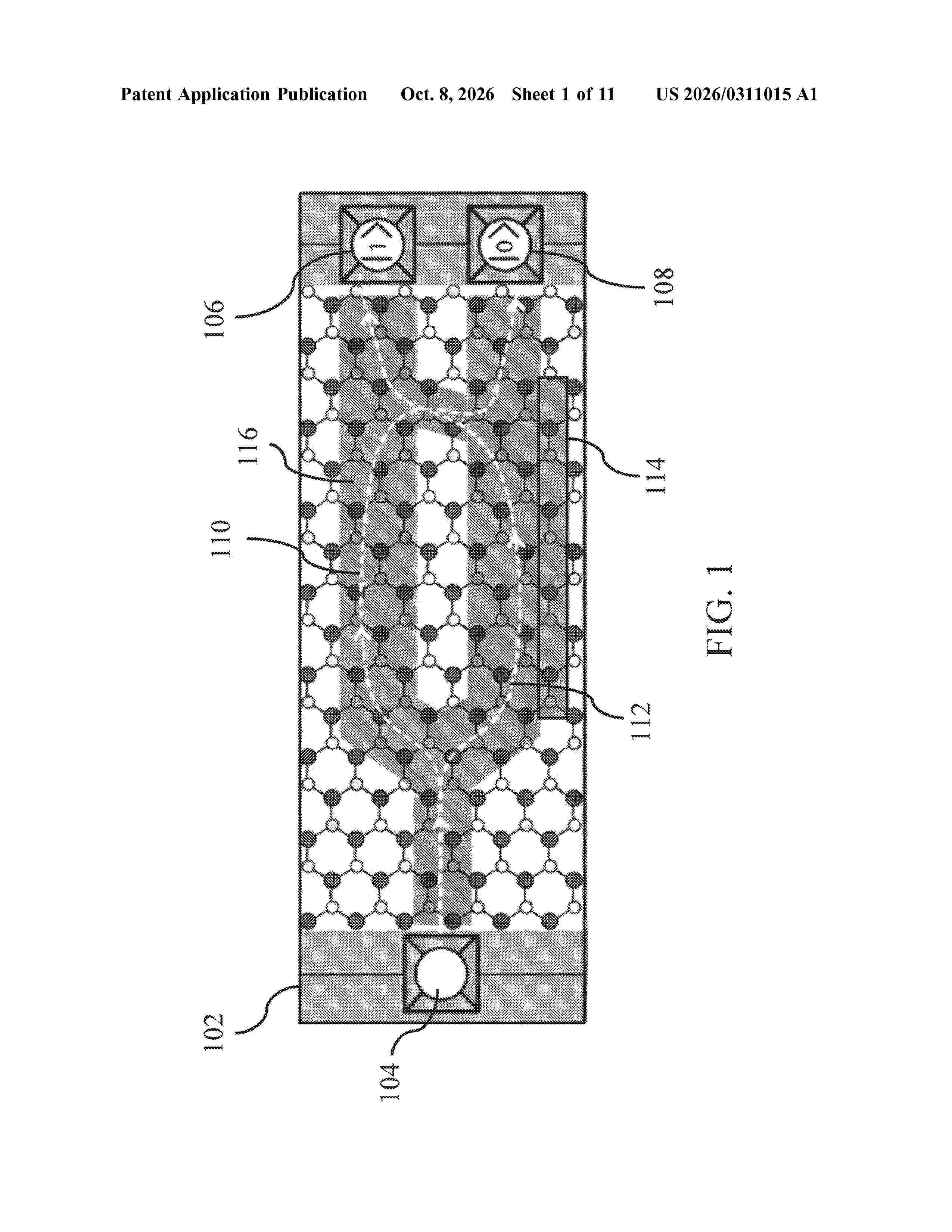
Resumen de: US20260311015A1
A method of optimizing a network-based quantum computer includes coupling a plurality of contacts with a network of transport channels. The plurality of contacts includes at least one read-out contact and at least one electrostatic control contact, and each channel of the network of transport channels is coupled with a read-out contact and an electrostatic control contact. The at least one electrostatic control contact is operable to control an electric charge within the network of transport channels. The method further includes initiating an optimization algorithm coupled with the plurality of contacts to generate an optimal contact setting configuration for the plurality of contacts coupled with the network of transport channels. Additionally, the method includes adjusting the plurality of contacts according to optimal the contact setting configuration.
Nº publicación: DE102025133101A1 08/10/2026
Solicitante:
DEUTSCH ZENTR LUFT & RAUMFAHRT [DE]
Deutsches Zentrum f\u00FCr Luft- und Raumfahrt e.V.
Resumen de: DE102025133101A1
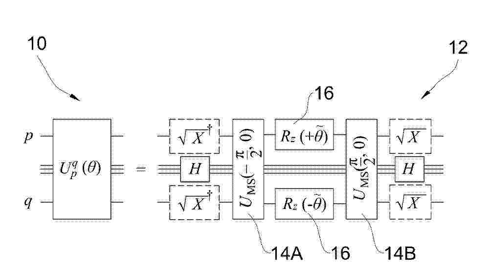
Quantenschaltkreis zur Anwendung eines Anregungsoperators auf ein fermionisches System zur Erzeugung eines Zielzustands mit einer Vielzahl von Qubits, wobei das fermionische System mindestens ein Ausgangsorbital und mindestens ein Zielorbital aufweist, wobei eine Anregung von dem Ausgangsorbital in das Zielorbital durch den Anregungsoperator erfolgen soll, wobei ein Ausgangs-Qubit p das Ausgangsorbital und Ziel-Qubit q das Zielorbital repräsentiert, mindestens ein erstes globales Gatter und mindestens ein zweites globales Gatter, welche jeweils gemeinsam zumindest auf das Ausgangs-Qubit p und das Ziel-Qubit q wirken, eine erste z-Rotation und eine zweite z-Rotation, die zwischen dem ersten globalen Gatter und dem zweiten globalen Gatter angeordnet sind und parallel jeweils auf das Ausgangs-Qubit p und das Ziel-Qubit q wirken, wobei durch das erste globale Gatter, das zweite globale Gatter, die erste z-Rotation und die zweite z-Rotation mindestens zwei Pauli-Rotationen des Anregungsoperators parallelisiert ausgeführt werden zur Erzeugung des Zielzustands.
 BOPI
 Sede Electrónica