Si deseas distinguir tus productos, servicios o ambos de los de otra empresa, es posible que necesites una marca o nombre comercial. Descubre qué son, en qué consiste su procedimiento de registro y qué implica.

Información sobre los plazos de presentación de solicitudes de transformación de marcas de la Unión Europea en marca nacional española. Más información


Si tienes un nuevo dispositivo, producto o procedimiento que resuelva un problema técnico o tenga una ventaja práctica, existen distintas formas de protegerlo en España y en otros países. Descubre cómo hacerlo.

¿Tu innovación reside en la estética, la ornamentación o la apariencia de tu producto? Protégela mediante un diseño industrial. Descubre qué derechos confiere el registro y cómo realizar la tramitación.

Las indicaciones geográficas protegen el nombre de un producto originario de una zona geográfica, a la cual le debe una determinada calidad, reputación u otra característica. Descubre qué son, en qué consiste su procedimiento de registro y qué beneficios conceden.

Las patentes publicadas en todo el mundo son una valiosa fuente de información científica, técnica y comercial.

Si eres emprendedor/a o una empresa y quieres potenciar y mejorar la rentabilidad de tu negocio protegiendo de forma adecuada los activos intangibles de tu organización, en este espacio encontrarás lo necesario.


 224
resultados
224
resultados
 Última actualización
23/10/2026 [09:45:00]
Última actualización
23/10/2026 [09:45:00]


 Resultados 125 a 150 de 224

Resumen de: WO2025120077A1
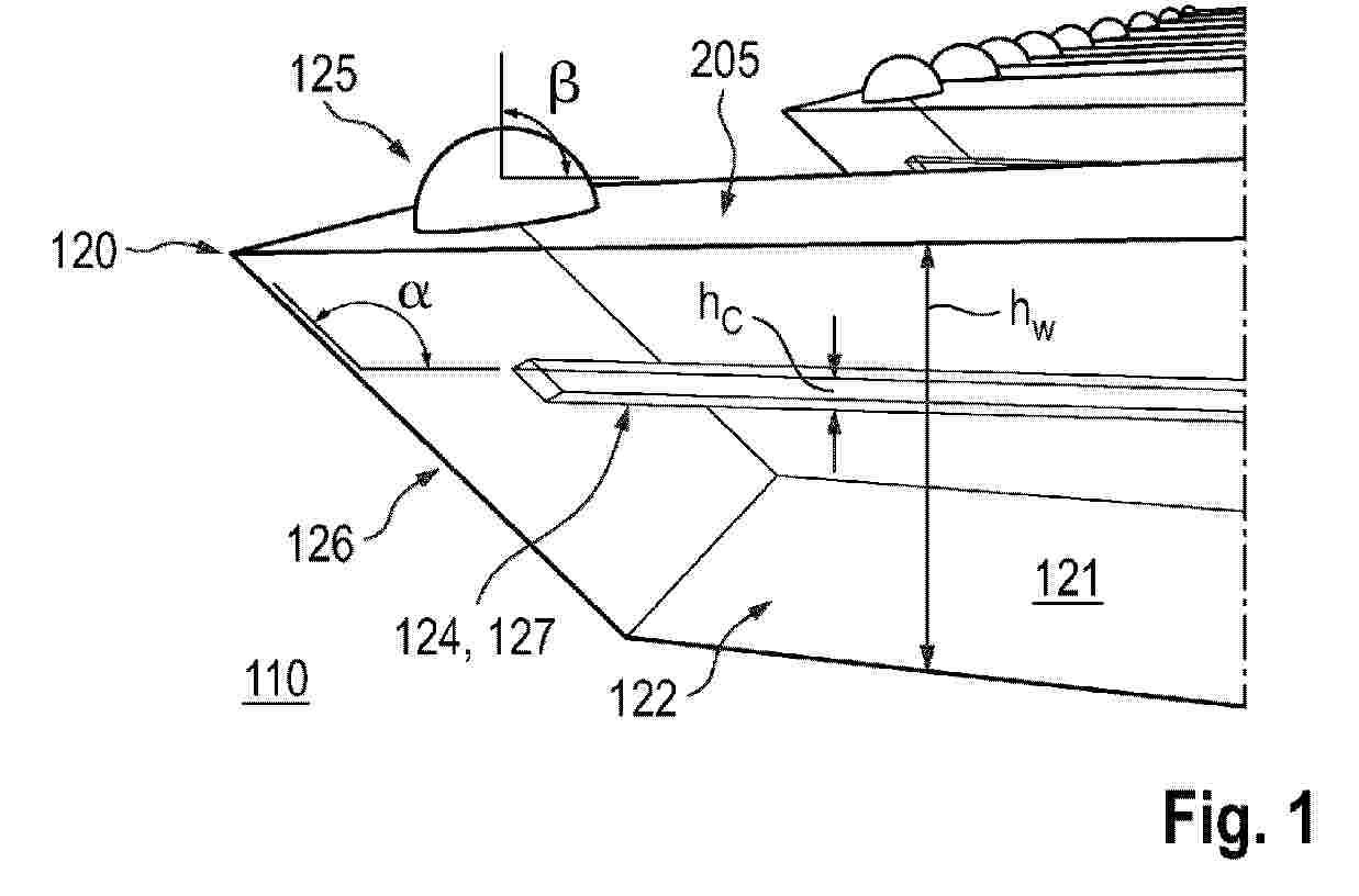
An optical system (100) for controlling the state of an ion in a Paul trap (201), the optical system (100) comprising: - a substrate (110) adapted to be coupled to the Paul trap (201); - at least one waveguide (120) formed on and/or in the substrate (110), wherein the waveguide (120) comprises a main body (121), the main body (121) having a waveguide facet (126) at an end of the main body (121) of the waveguide (120), the waveguide facet (126) having a deflection angle (α) configured to guide light from the waveguide (120) through a main surface (205) of the main body (121) of the wave guide (120) to an ion in the Paul trap (201).

Resumen de: WO2025064374A1
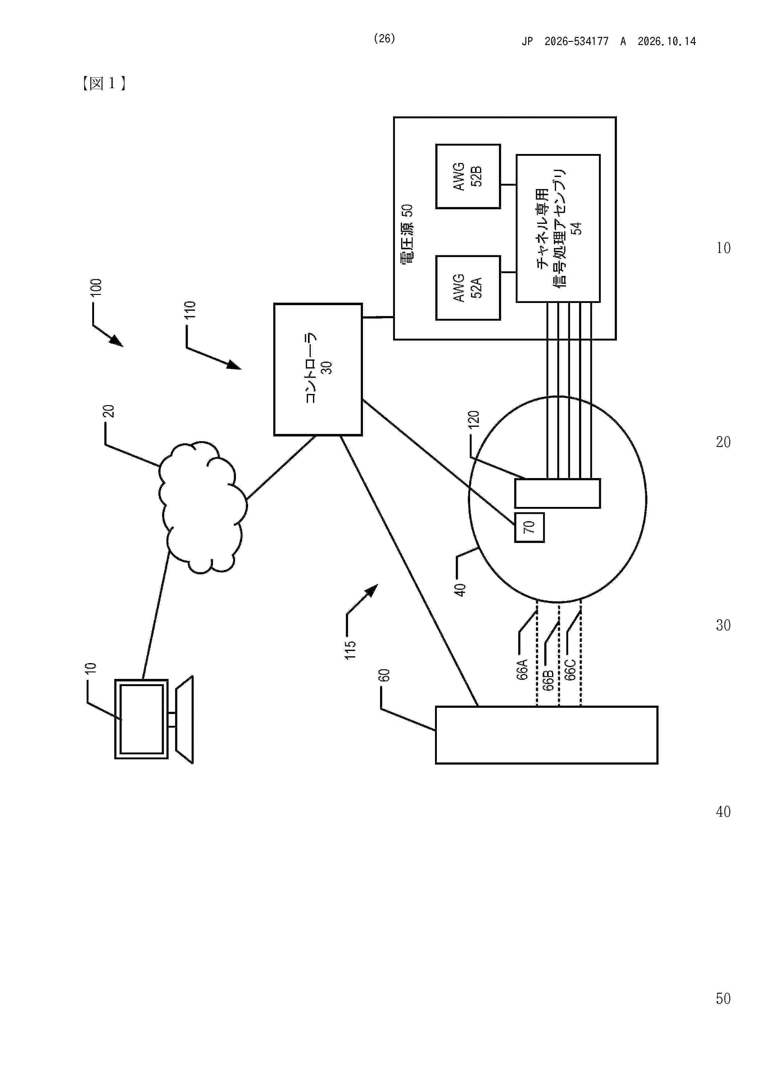
A system includes a confinement apparatus, arbitrary waveform generators (AWGs), and channel-dedicated signal processing assemblies. Application of respective voltage signals to the plurality of control electrodes of the confinement apparatus is configured to cause the confinement apparatus to confine manipulatable objects. The AWGs are operable to generate respective waveforms. Each signal processing assembly is configured to condition a voltage signal applied to a respective electrode of the confinement apparatus. The signal processing assembly includes a channel-dedicated voltage generator and an operational amplifier. The operational amplifier is configured to receive (i) a broadcasted waveform generated by an AWG and broadcasted to at least two signal processing assemblies of the plurality of channel -dedicated signal processing assemblies and (ii) a quasi-static voltage generated by the channel-dedicated voltage generator. The operational amplifier is configured to output a combined signal generated by combining the broadcasted waveform and the quasi-static voltage.
Resumen de: WO2025058895A2
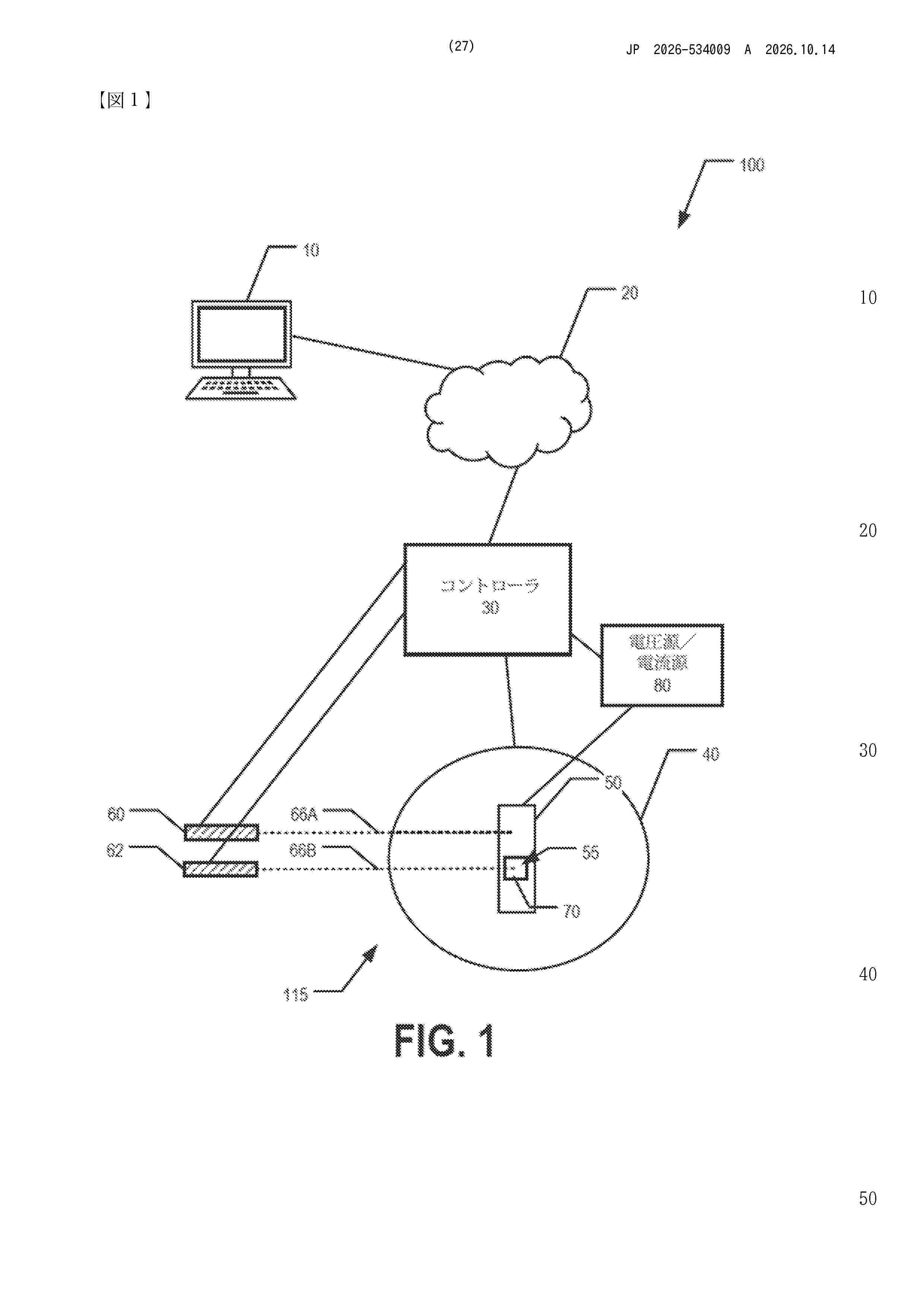
A controller of a quantum system causes performance of a single qubit gate on a target qubit. The controller causes a dressing field circuit to generate a dressing field at a target location where the target qubit is located. The dressing field modifies a set of initial states into a set of superposition states. A first (second) dressed state of the set of superposition states includes a non-zero contribution from a first (second) qubit state of the set of initial states. A dressed frequency difference between the first and second dressed states and a qubit frequency difference between the first and second qubit states are different. The controller causes a gate microwave signal characterized by the dressed frequency difference plus the qubit frequency difference to be incident on the target location. After a gate time, the controller controls operation of the dressing field circuit to stop generating the dressing field.
Resumen de: EP4822563A1
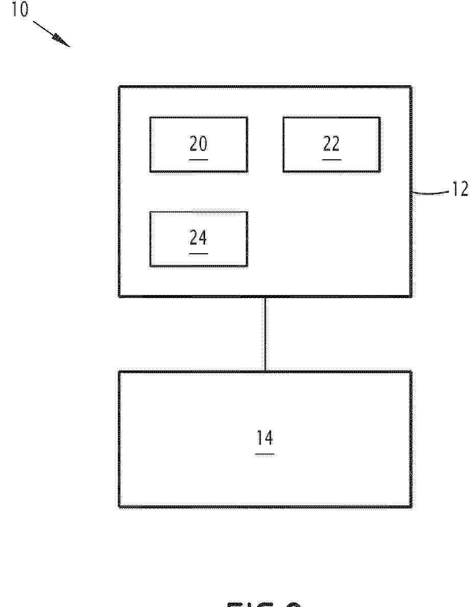
0001 The invention relates to a method for characterizing the imaging fidelity of an imaging unit (22) of a quantum device (12), the imaging unit (22) being suitable to acquire images of a quantum register generated by the quantum device (12), and to detect, on the acquired images, particles trapped in trapping sites of the quantum register as a function of a given detection threshold, the detection threshold being such that, for each trapping site, a particle is considered present in said trapping site when the number of electrons, resulting from the conversion of the photons received by the imaging unit (22) at the location of said trapping site, is above the detection threshold, and being considered absent otherwise, the method being implemented by a computing system (10) comprising the quantum device (12) and a classical computer (14).
Resumen de: EP4822611A1
The method can include computing a leading-order error operator based on fragments of a Hamiltonian representing the one more molecules, where the fragments can be diagonalized, and a product formula approximating the time evolution; computing a set of eigenstates representing a classical solution of the Hamiltonian; computing product formula expectation values of the leading-order error operator for at least some eigenstates of the set; computing a maximum time step associated to a target error using the product formula expectation values; and performing a quantum phase estimation quantum computing process to determine the spectrum, including performing one or more Fourier transforms of the product of the distribution with the one or more expectation values in a discretized manner, over one or more time steps, the one or more time steps being equal to or lesser than the maximum time step.
Resumen de: EP4822610A1
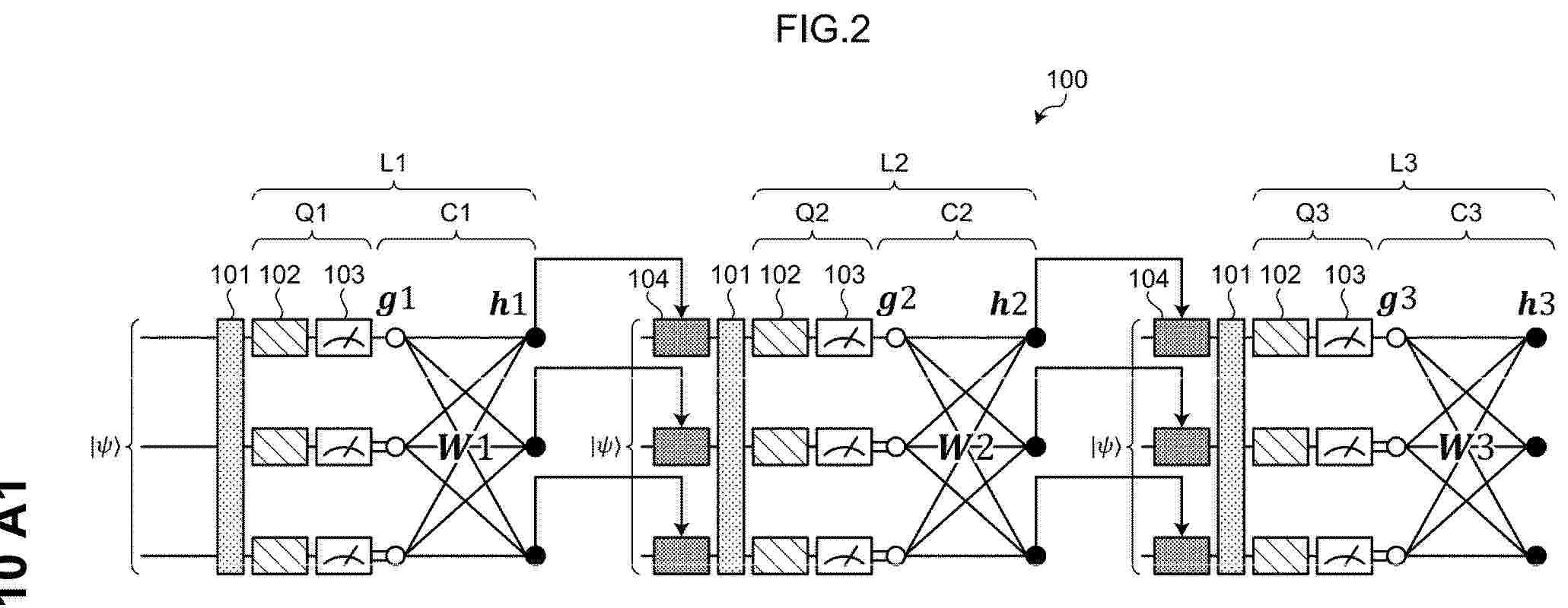
0001 An information processing program causes a computer to execute a process including, in a machine learning model configured to have layers, an input of quantum data being accepted at a first layer, a preceding layer of two consecutive layers included in the layers inputting an output generated by the generation function based on an output of the quantum circuit to the quantum circuit included in a subsequent layer, inputting first quantum data to the first layer and causing first output data to be generated, and inputting, in each second layer arranged in a subsequent stage to the first layer, second quantum data to a quantum circuit that has generated a quantum feature map for an output from a layer arranged in a preceding stage of each second layer, and causing second output data to be generated.
Resumen de: EP4822612A1
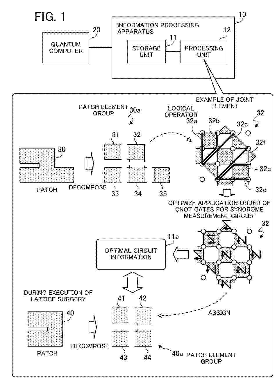
0001 A processing unit identifies a first joint element from a first patch element group included in a first patch that appears in the course of lattice surgery, performs an optimization process for optimizing an application order of controlled NOT (CNOT) gates for a syndrome measurement circuit in the first joint element with respect to a direction of a logical operator defined for the first joint element, and stores, in a storage unit, optimal circuit information associating the first joint element with the application order of CNOT gates. The processing unit identifies, upon detecting a second path during execution of lattice surgery, a second joint element corresponding to the first joint element from a second patch element group included in the second patch, and assigns the application order of CNOT gates associated with the first joint element to the second joint element, based on the optimal circuit information.
Resumen de: EP4822592A1
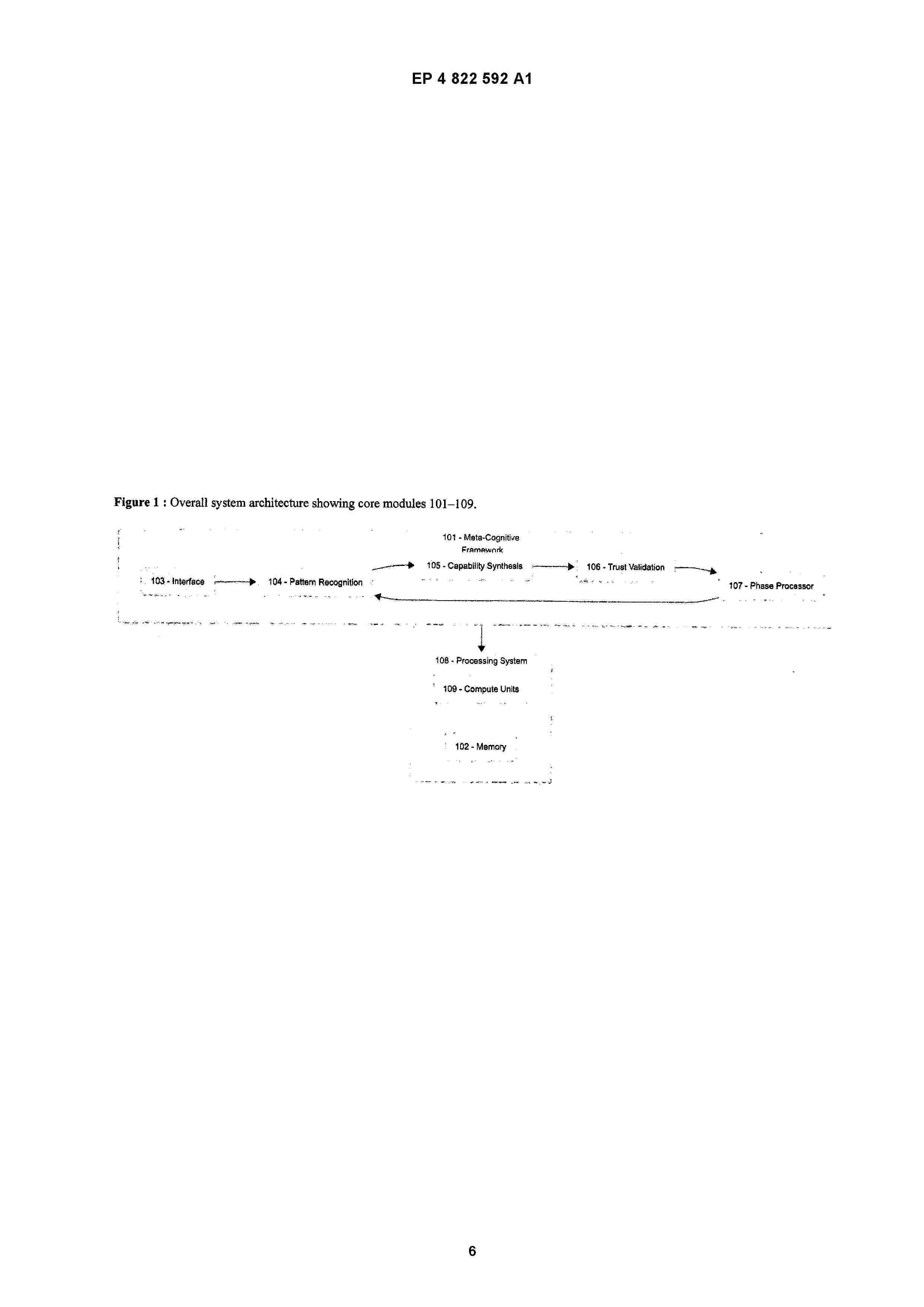
0001 A meta-cognitive AI framework employing quantum-inspired algorithms is disclosed for adaptive pattern recognition on classical computing hardware. The system uses complex phase-space transformations, O(n<2>) Lanczos eigenvalue computation, and deterministic interference synthesis with 128-dimensional complex vectors. Emergent capabilities are identified through residual projection analysis and validated via adaptive threshold control. The invention improves recognition accuracy, processing efficiency, and adaptability across industrial domains such as robotics, healthcare, environment, energy , transport, defence, space and finance. It represents a novel integration of meta-cognitive feedback, quantum-inspired computation, and emergence detection not previously combined in prior art.
Resumen de: WO2025191211A1
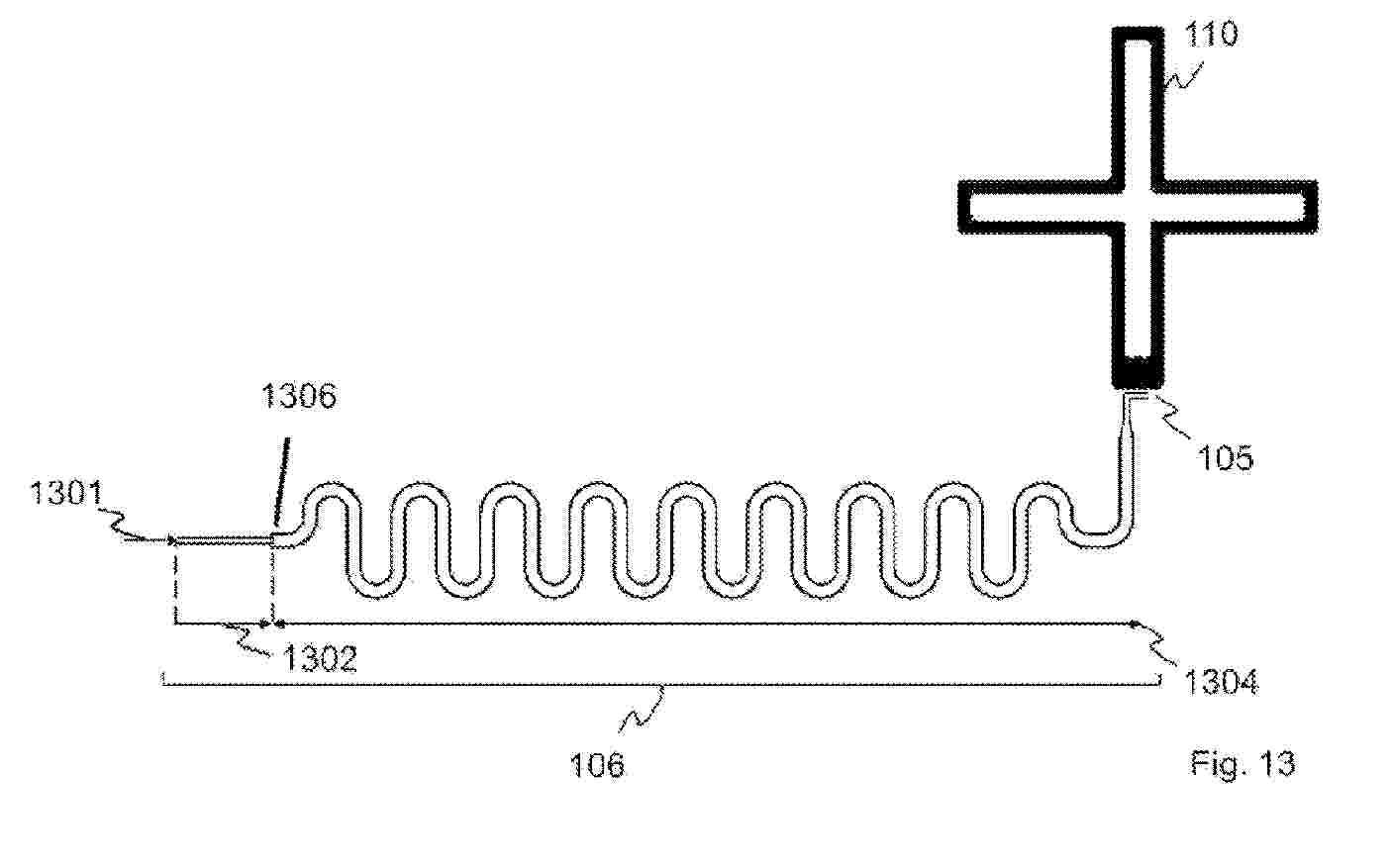
There is provided mitigating Purcell loss at qubit frequency. A flux line for manipulating at least one qubit, comprises: a first segment (1302) for connecting to an input terminal for receiving a control signal; and a second segment (1304, 1604) for coupling the control signal to a Superconducting Quantum Interference Device (SQUID) operatively connected to the at least one qubit, the second segment is arranged consecutive with respect to the first segment (1302), and the first segment and the second segment are configured to have an impedance mismatch at a qubit frequency of the at least one qubit.
Resumen de: WO2025195741A2
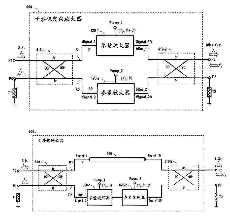
A device comprises a superconducting parametric interferometric circuit, which comprises a signal input port and a signal output port, and a first parametric mixing circuit and a second parametric mixing circuit coupled in parallel between the signal input port and the signal output port. The signal input port configured to receive an input signal having a first frequency. The first parametric mixing circuit is configured to convert the input signal to a first output signal having a second frequency, and the second parametric mixing circuit is configured to convert the input signal to a second output signal having the second frequency. The superconducting parametric interferometric circuit is configured to constructively combine the first and second output signals at the signal output port to generate an output signal having the second frequency, and provide isolation of the signal input port from a signal which is present at the signal output port.
Resumen de: CN122905092A
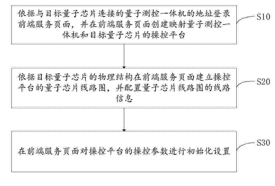
本申请公开了一种量子测控软件系统的初始化方法、运行方法及量子计算机,属于量子计算技术领域;初始化方法应用于提供前端服务页面的量子测控软件系统,方法包括:依据与目标量子芯片连接的量子测控一体机的地址登录前端服务页面,并在前端服务页面创建映射量子测控一体机和目标量子芯片的操控平台;依据目标量子芯片的物理结构在前端服务页面建立操控平台的量子芯片线路图,并配置量子芯片线路图的线路信息;在前端服务页面对操控平台的操控参数进行初始化设置。本申请通过在前端服务页面对操控平台中的量子芯片和量子测控一体机的相关参数进行配置,以实现操控平台的初始化初始化,提高效率。
Resumen de: CN122905086A
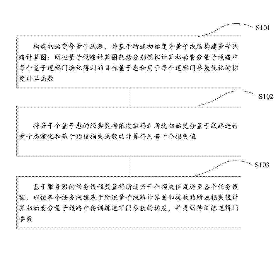
本发明涉及量子神经网络技术领域,具体涉及一种加速变分量子线路训练的方法、装置及量子计算机,本申请通过构建量子线路计算图结合变分量子线路进行正向传播和损失函数计算得到的若干个损失值,在经典计算机上实现对变分量子线路反向梯度的计算,无需进行多次变分量子线路的反向梯度计算,避免变分量子线路反向梯度计算耗时较长的问题,同时将若干个量子态的经典数据划分到经典计算机其他计算节点的任务线程上进行分布式计算,进一步加速了整个变分量子线路训练过程。
Resumen de: CN122905091A
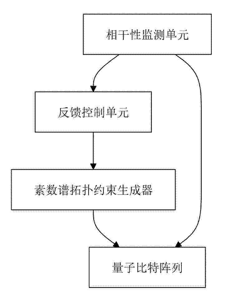
本发明公开了一种基于素数谱拓扑约束的量子比特相干调控芯片。所述芯片包括量子比特阵列、素数谱拓扑约束生成器、相干性监测单元和反馈控制单元。素数谱拓扑约束生成器在量子比特上施加满足素数谱流形拓扑约束的相干调控脉冲序列,相干性监测单元实时监测相干时间,反馈控制单元动态调整脉冲参数。本发明可应用于量子比特的相干时间延长、退相干抑制和量子门操作的保真度提升。
Resumen de: CN122905087A
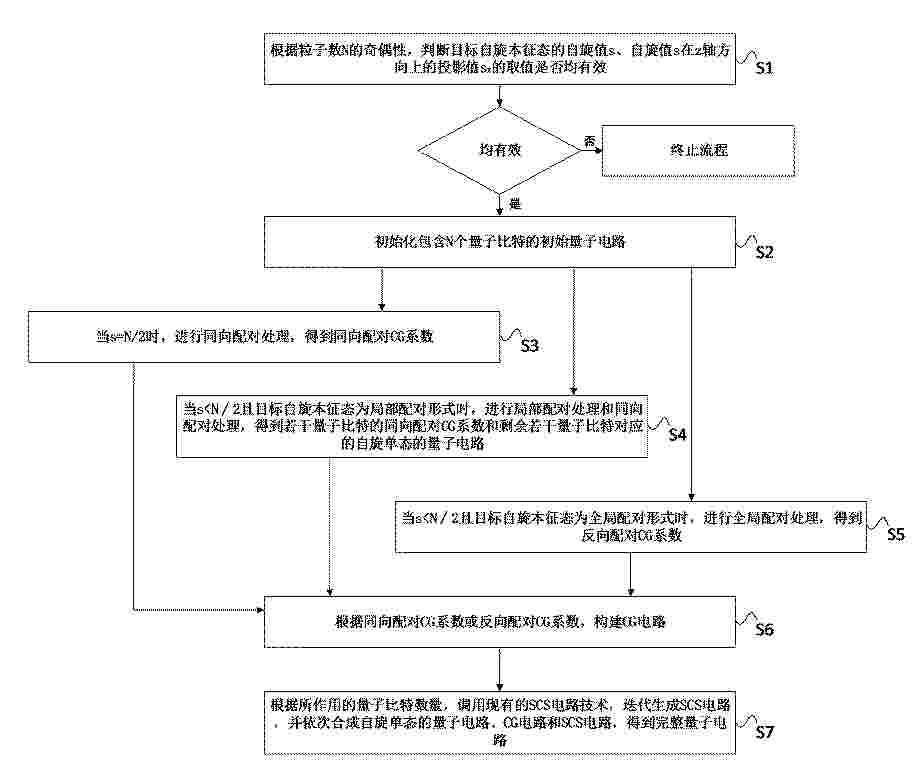
本发明公开了一种制备特殊自旋本征态的量子电路构建方法和系统,本发明的方法包括:根据粒子数的奇偶性,判断目标自旋本征态的自旋值、自旋值在轴方向上的投影值的取值是否均有效;若均有效,则初始化包含个量子比特的初始量子电路;当时,进行同向配对处理,得到同向配对CG系数;当且目标自旋本征态为局部配对形式时,进行局部配对处理和同向配对处理,得到若干量子比特的同向配对CG系数和剩余若干量子比特对应的自旋单态的量子电路;当且目标自旋本征态为全局配对形式时,进行全局配对处理,得到反向配对CG系数;构建CG电路。本发明能够有效控制量子电路深度和量子门数量,保证制备效率。
Resumen de: CN122903767A
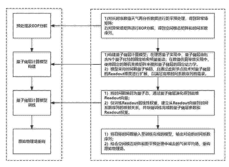
本发明公开了一种基于量子储层计算的长时序数值天气再分析数据压缩与检索方法及系统,应用于量子计算与气象应用的交叉技术领域,包括:对长时序数值天气再分析数据进行EOF分解;构建量子储层计算模型;在理想量子实现中,量子储层由包含个量子比特的固定哈密顿量驱动;且通过虚拟节点技术对量子储层的Readout维度进行扩展;将时间戳编码为量子态,仅训练Readout层线性权重,建立从Readout向量到时间系数序列的映射关系;将目标时间戳输入至训练完成的模型,输出对应的时间系数序列,并结合空间模态矩阵和气候平均场,重构原始物理场。本发明实现了任意时间戳的随机访问,且兼具高压缩比、高精度和低训练成本。
Resumen de: CN122903757A
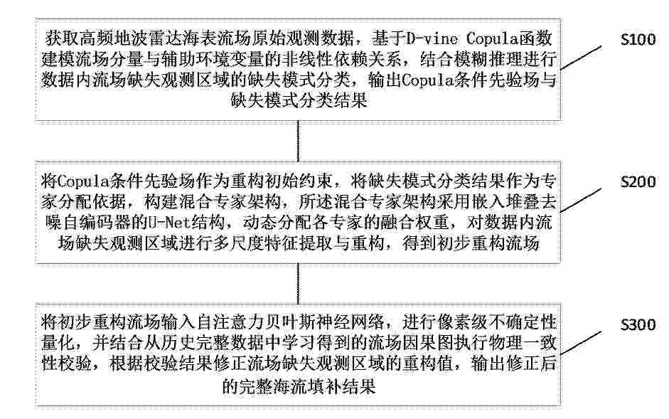
本发明公开了一种高频地波雷达海流观测填补拓延方法及系统,该方法包括:基于D‑vine Copula函数建模流场分量与辅助环境变量的非线性依赖关系,结合模糊推理完成流场缺失观测区域的模式分类,输出Copula条件先验场与缺失模式分类结果;再以先验场为重构初始约束、分类结果为专家分配依据,通过嵌入堆叠去噪自编码器的混合专家U‑Net架构,对缺失区域做多尺度特征提取与重构,得到初步重构流场;最后经自注意力贝叶斯网络完成像素级不确定性量化,结合流场因果图执行物理一致性校验与修正,输出完整海流填补结果。本发明能够提高缺失流场数据的保真度与可预测性。本发明作为一种高频地波雷达海流观测填补拓延方法及系统,可广泛应用于海表流场数据处理技术领域。
Resumen de: CN122905085A
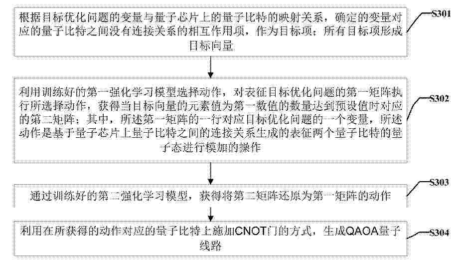
本申请公开了一种QAOA量子线路生成方法、装置、设备及介质,属于量子计算技术领域,方法包括:根据目标优化问题的变量与量子芯片上的量子比特的映射关系,确定的变量对应的量子比特之间没有连接关系的相互作用项,作为目标项;所有目标项形成目标向量;利用训练好的第一强化学习模型选择动作,对表征目标优化问题的第一矩阵执行所选择动作,获得当目标向量的元素值为第一数值的数量达到预设值时对应的第二矩阵;其中,所述第一矩阵的一行对应目标优化问题的一个变量,所述动作是基于量子芯片上量子比特之间的连接关系生成的表征两个量子比特的量子态进行模加的操作;通过训练好的第二强化学习模型,获得将第二矩阵还原为第一矩阵的动作;利用在所获得的动作对应的量子比特上施加CNOT门的方式,生成QAOA量子线路。应用本申请实施例,可以减少实现QAOA所占用的量子资源。
Resumen de: CN122905095A
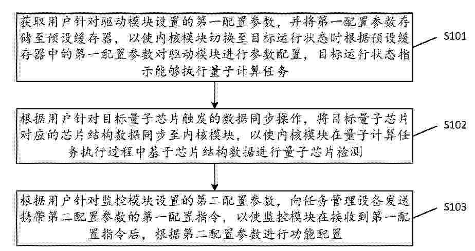
本申请实施例提供了一种设备初始化方法、前端服务设备及存储介质。方案如下:获取第一配置参数,并将第一配置参数存储至预设缓存器,以使内核模块切换至目标运行状态时根据第一配置参数对驱动模块进行参数配置;根据用户触发的数据同步操作,将目标量子芯片对应的芯片结构数据同步至内核模块,以使内核模块在量子计算任务执行过程中基于芯片结构数据进行量子芯片检测;根据用户针对监控模块设置的第二配置参数,向任务管理设备发送携带第二配置参数的第一配置指令,以使监控模块在接收到第一配置指令后,根据第二配置参数进行功能配置。通过本申请实施例提供的技术方案,实现了设备管理模块的初始化,为后期量子计算任务的正常执行提供保障。
Resumen de: CN122905088A
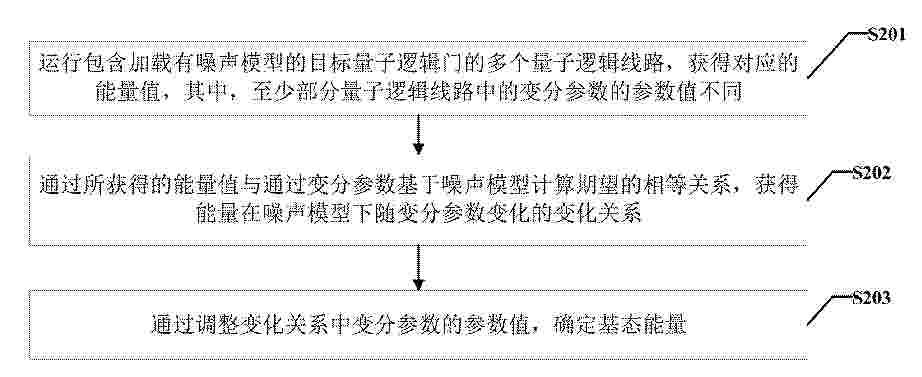
本申请公开了一种量子模拟方法、装置、设备及介质,属于量子计算技术领域,方法包括:运行包含加载有噪声模型的目标量子逻辑门的多个量子逻辑线路,获得对应的能量值,其中,至少部分量子逻辑线路中的变分参数的参数值不同;通过所获得的能量值与通过变分参数基于噪声模型计算期望的相等关系,获得能量在噪声模型下随变分参数变化的变化关系;通过调整变化关系中变分参数的参数值,确定基态能量。应用本申请实施例,可以减少计算资源的耗费。
Resumen de: CN122905090A
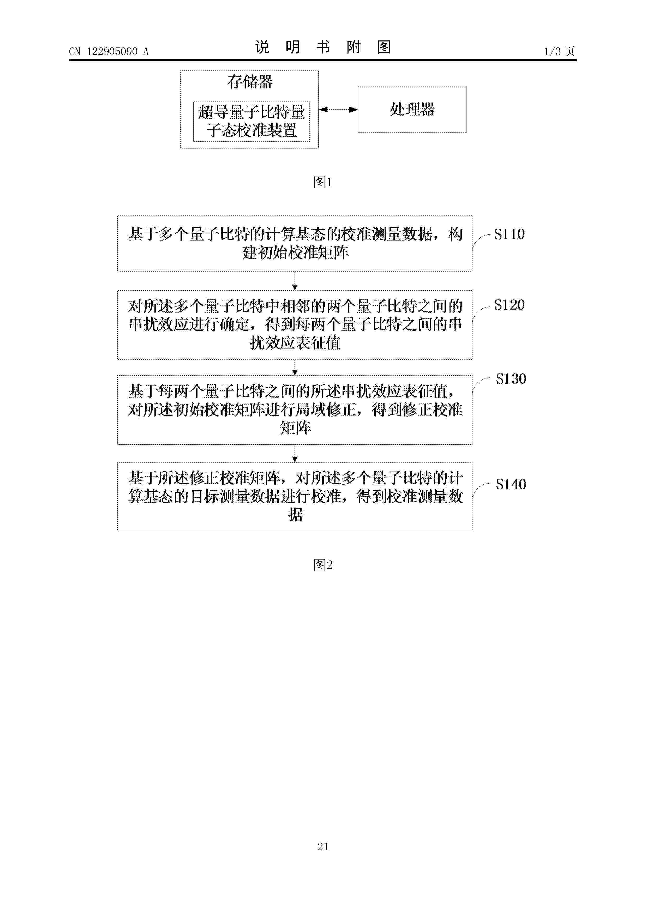
本申请提供的超导量子比特量子态校准方法和装置、设备及介质,涉及量子计算技术领域。在本申请中,首先,基于多个量子比特的计算基态的校准测量数据,构建初始校准矩阵,其中,初始校准矩阵中的第y行、第x列的元素用于表示:当真实态为x时,测量数据被读成y的概率;其次,对多个量子比特中相邻的两个量子比特之间的串扰效应进行确定,得到量子比特之间的串扰效应表征值;然后,基于每两个量子比特之间的串扰效应表征值对初始校准矩阵进行局域修正,得到修正校准矩阵;最后,基于修正校准矩阵对目标测量数据进行校准,得到校准测量数据。基于上述内容,可以改善现有技术中存在的难以对测量数据进行有效校准的问题。
Resumen de: CN122905084A
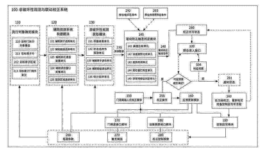
本申请公开了一种中性原子量子门的非破坏性观测与联动校正方法及系统。该方法包括:获取量子门执行序列中的目标门执行对象集合;构建与目标门执行对象集合在空间位置、能级结构、同位素类型、跃迁通道、读出窗口、读出波段、控制光路或光场作用区域中的至少一项相隔离的辅助观测系统;在门后检测窗口、门序列间窗口、相邻量子门执行间隔或者批次级观测窗口中,通过辅助观测系统获取与目标门执行过程相关的观测数据;基于观测数据、阈值、误差预算、相关性条件或者异常持续性条件生成联动校正触发信号;根据观测采集时间、触发判定时间、控制指令下发时间和目标门下一执行时间确定预设插入窗口及校正许可状态;在校正许可状态满足时于预设插入窗口内插入校正操作,在校正许可状态不满足时转入批次级校正、重新标定或者控制面回写;并基于校正后门执行结果更新观测参数、触发阈值或者校正控制参数。本申请不以破坏目标门执行对象集合主量子态的读出结果作为联动校正触发信号来源,有利于形成受插入窗口和时延预算约束的门控校正闭环。
Resumen de: CN122909184A
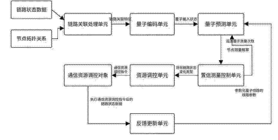
本发明公开一种基于量子机器学习的分布式智能通讯系统,涉及量子计算与分布式通信技术领域,链路关联处理单元根据链路状态数据时序变化及拓扑相邻节点状态差异构建链路关联特征;量子编码单元将其映射为量子旋转参数,按节点拓扑关系设置受控纠缠关系,形成量子输入状态;量子预测单元利用参数化量子线路获得各候选链路状态变化类型的节点测量概率;置信测量控制单元根据节点测量概率、量子测量次数及节点间概率差异确定综合不确定度和概率区间,并根据更新后的概率区间确定目标链路状态变化类型;资源调控单元据此生成通信资源调控指令并输出至通信资源调控对象。本发明提高链路状态判定与资源调控可靠性。
Resumen de: CN122905093A
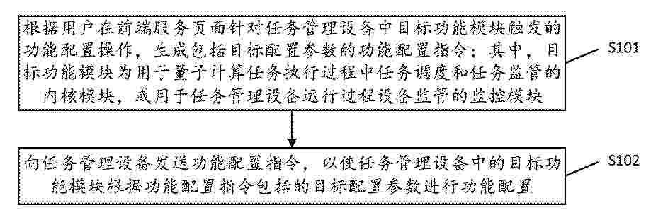
本申请实施例提供了一种功能配置方法及前端服务设备。方案如下:根据用户在前端服务页面针对任务管理设备中目标功能模块触发的功能配置操作,生成包括目标配置参数的功能配置指令;其中,目标功能模块为用于量子计算任务执行过程中任务调度和任务监管的内核模块,或用于任务管理设备运行过程设备监管的监控模块;向任务管理设备发送功能配置指令,以使任务管理设备中的目标功能模块根据功能配置指令包括的目标配置参数进行功能配置。通过本申请实施例提供的技术方案,可以通过前端服务页面实现任务管理设备的功能配置。
Resumen de: CN122908329A
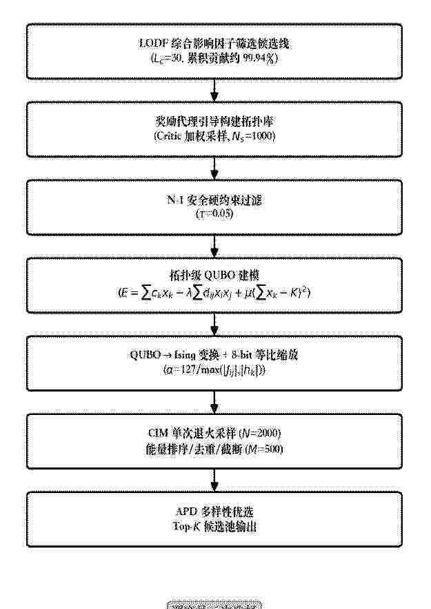
本公开提供了基于量子相干伊辛机采样的电网拓扑候选优化方法及系统,涉及电力系统运行控制与量子计算交叉技术领域,包括:训练奖励代理网络引导构建高效拓扑库;以N‑1安全裕度为硬约束过滤拓扑;以“拓扑是否入选候选池”为决策变量构造QUBO目标函数,经伊辛变换与8‑bit等比缩放后提交相干伊辛机,由单次退火并行产出多个低能态样本;经能量排序、去重、截断与基数修复后,以池内平均成对汉明距离为多样性准则优选候选池输出。本公开将相干伊辛机从“求最优”工具重新定位为“多样性候选集生成器”,一次性产出兼顾质量与多样性的候选池供调度员选择。本公开实现兼顾质量与多样性的候选池的快速生成。
Nº publicación: CN122908330A 13/10/2026
Solicitante:
南京理工大学
Resumen de: CN122908330A
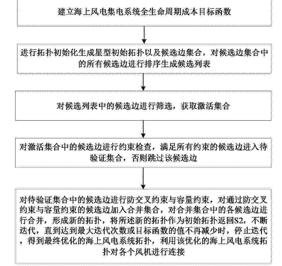
本发明公开了一种海上风电集电系统拓扑优化方法及系统,方法包括:建立海上风电集电系统全生命周期成本目标函数;进行拓扑初始化生成初始拓扑以及候选边集合;对候选列表中的候选边进行筛选,获取激活集合;对激活集合中的候选边进行约束检查,满足所有约束的候选边进入待验证集合,否则跳过该候选边;对待验证集合中的候选边进行防交叉约束与容量约束,对通过防交叉约束与容量约束的候选边加入合并集合,对合并集合中的各候选边进行合并,形成新的拓扑,得到最终优化的海上风电系统拓扑,利用该优化的海上风电系统拓扑对各个风机进行连接;本发明的优点在于:兼顾全生命周期成本优化、防交叉工程约束及全局搜索能力。
 BOPI
BOPI
 Sede Electrónica