Si deseas distinguir tus productos, servicios o ambos de los de otra empresa, es posible que necesites una marca o nombre comercial. Descubre qué son, en qué consiste su procedimiento de registro y qué implica.

Información sobre los plazos de presentación de solicitudes de transformación de marcas de la Unión Europea en marca nacional española. Más información


Si tienes un nuevo dispositivo, producto o procedimiento que resuelva un problema técnico o tenga una ventaja práctica, existen distintas formas de protegerlo en España y en otros países. Descubre cómo hacerlo.

¿Tu innovación reside en la estética, la ornamentación o la apariencia de tu producto? Protégela mediante un diseño industrial. Descubre qué derechos confiere el registro y cómo realizar la tramitación.

Las indicaciones geográficas protegen el nombre de un producto originario de una zona geográfica, a la cual le debe una determinada calidad, reputación u otra característica. Descubre qué son, en qué consiste su procedimiento de registro y qué beneficios conceden.

Las patentes publicadas en todo el mundo son una valiosa fuente de información científica, técnica y comercial.

Si eres emprendedor/a o una empresa y quieres potenciar y mejorar la rentabilidad de tu negocio protegiendo de forma adecuada los activos intangibles de tu organización, en este espacio encontrarás lo necesario.


 369
resultados
 Última actualización
22/11/2026 [07:15:00]


 Resultados 250 a 275 de 369

Resumen de: JP2026062763A
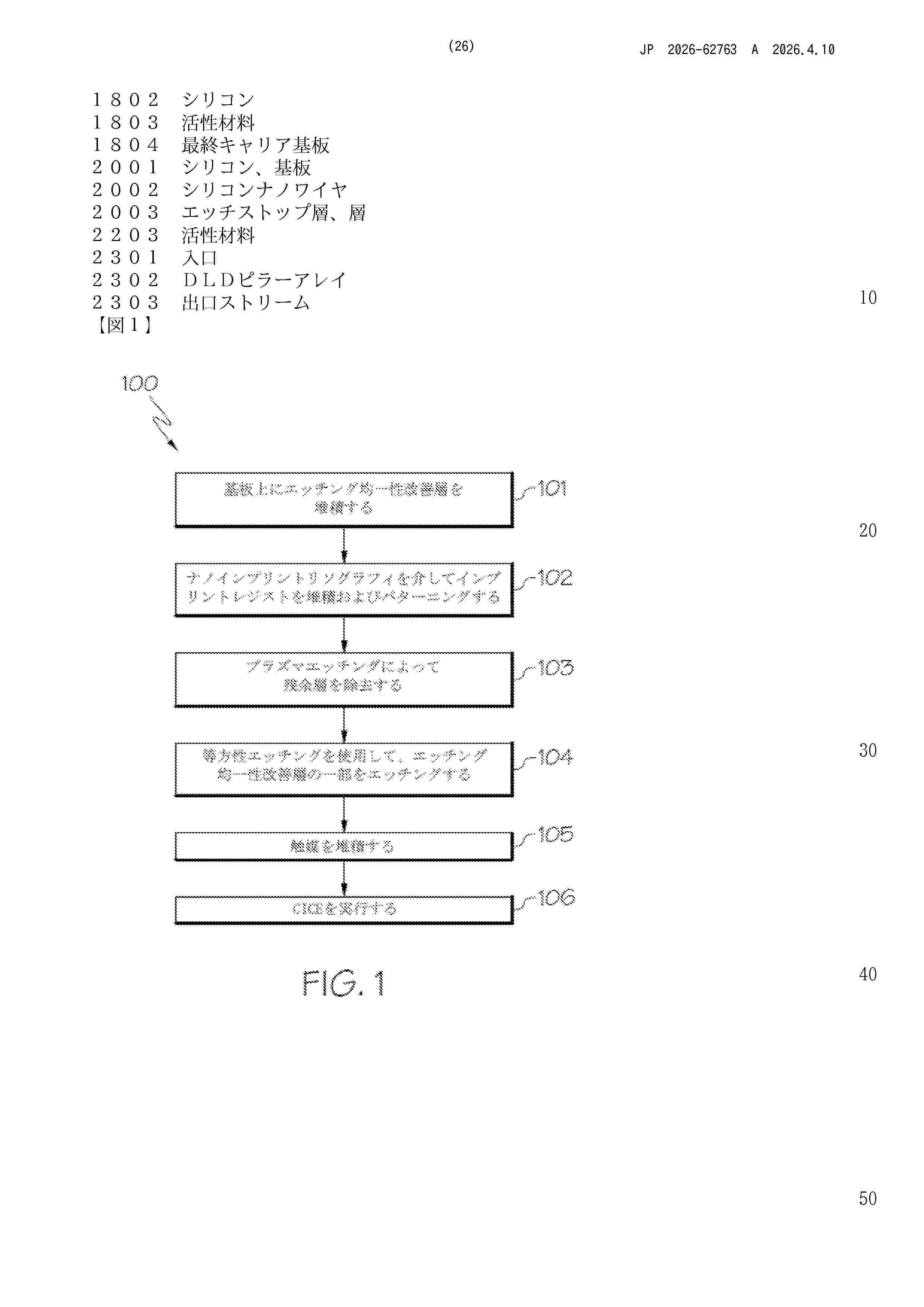
The present invention relates to catalyzed chemical etching.SOLUTION: A method for making a silicon nanostructure. An etch uniformity enhancement layer is deposited on the substrate. A catalyst (e.g., a thin film of Ti/Au) is deposited on the substrate or the etch uniformity enhancement layer, wherein the catalyst contacts a portion of the substrate or the etch uniformity enhancement layer. The catalyst and the substrate or the etch uniformity-enhancing layer are exposed to an etchant, wherein the catalyst causes etching of the substrate, thereby creating etched nanostructures.SELECTED DRAWING: Figure 1

Resumen de: US20260337342A1
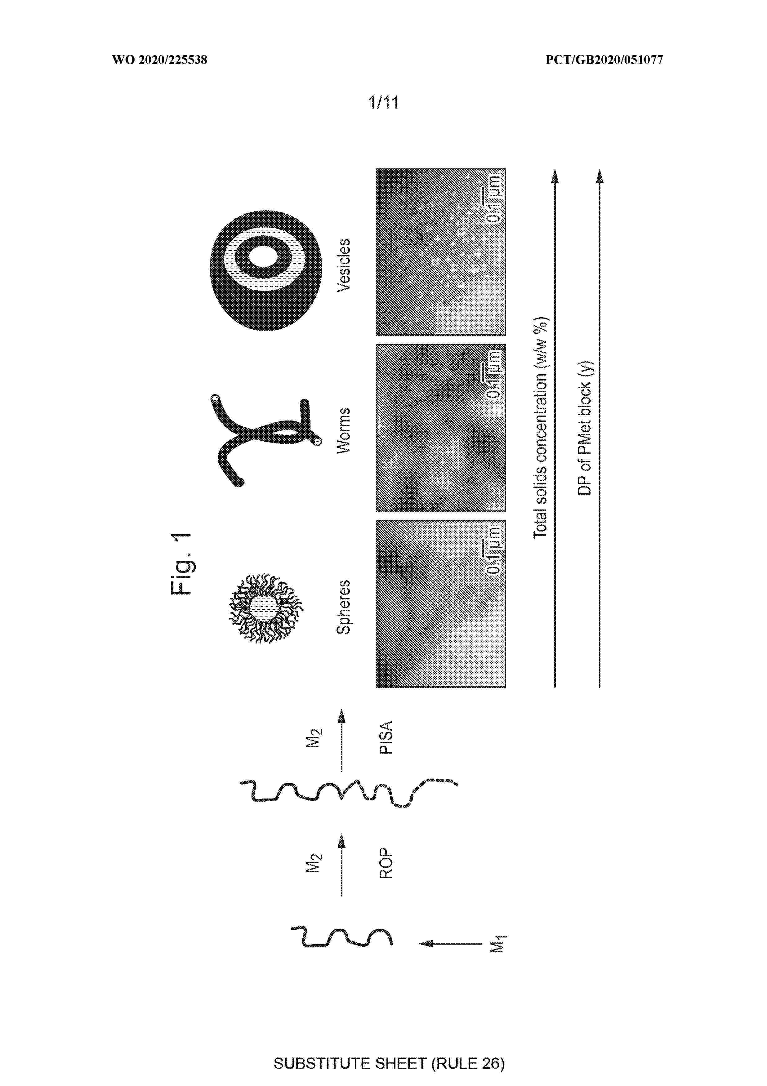
0000 The present invention is directed to a method for producing nanoparticles and microparticles composed of peptide- or peptoid-containing amphiphilic polymers. The method is simple, capable of achieving high yields, and can be tailored to produce a range of industrially and therapeutically useful structures including vesicles, micelles and hydrogels. The present invention also provides related hydrogels and vesicles having beneficial properties such an ability to degrade and release a payload in response to external stimuli.
Resumen de: US20260337047A1
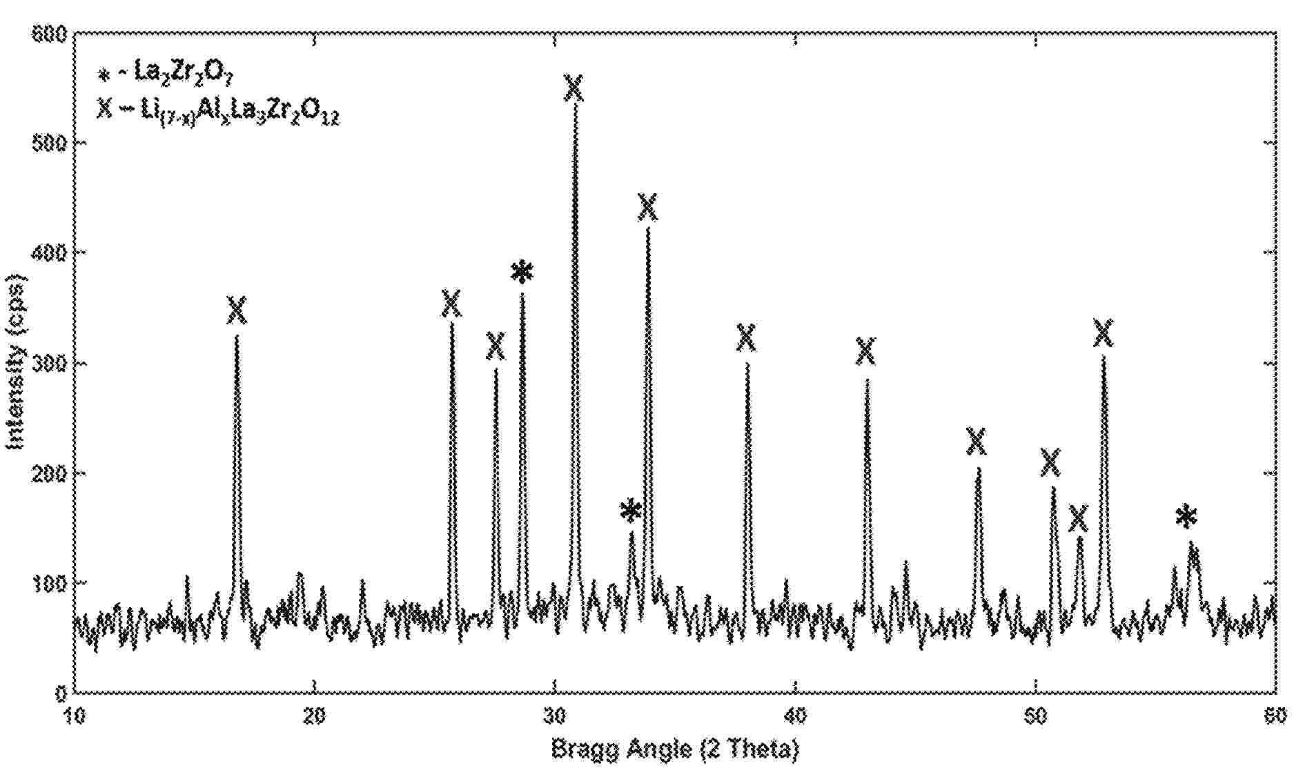
0000 Fabricating a layer including lithium lanthanum zirconate layer includes forming a slurry including lanthanum zirconate nanocrystals, a lithium precursor, and a lanthanum precursor in stoichiometric amounts to yield a dispersion including lithium, lanthanum, and zirconium. The slurry is dispensed onto a substrate and dried. The dried slurry is calcined to yield the layer including lithium lanthanum zirconate.
Resumen de: US20260344174A1
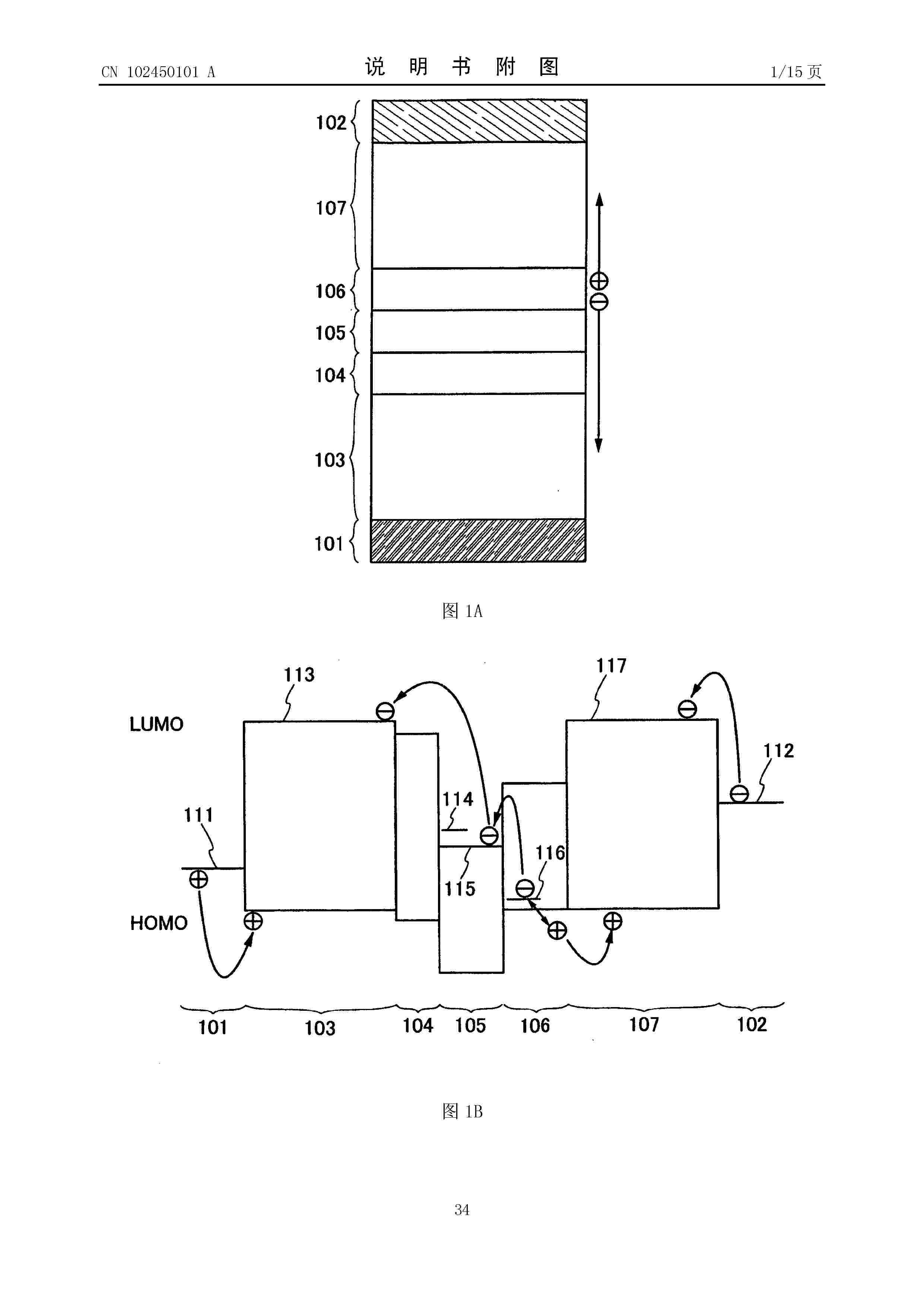
0000 An object is to provide a light-emitting element capable of emitting light with a high luminance even at a low voltage, and having a long lifetime. The light-emitting element includes n EL layers between an anode and a cathode (n is a natural number of two or more), and also includes, between m-th EL layer from the anode and (m+1)-th EL layer (m is a natural number, 1≤m≤n−1), a first layer including a first donor material in contact with the m-th EL layer, a second layer including an electron-transport material and a second donor material in contact with the first layer, and a third layer including a hole-transport material and an acceptor material in contact with the second layer and the (m+1)-th EL layer.
Resumen de: GB2705653A
A method of preparing a dispersion of carbon nanomaterials is disclosed which comprises a first dispersing step, in which a carbon nanomaterial is mixed in a solvent with a first portion of dispersant; a deagglomeration step, in which the resulting mixture is subjected to a deagglomeration treatment so as to reduce agglomeration of particles of the carbon nanomaterial within the mixture; and a second dispersing step, in which a second portion of dispersant is added to the mixture and the mixture is further mixed to form the dispersion. The dispersant may be carboxymethyl cellulose. Figure 1
Resumen de: KR20260156168A
본 발명은 AIC(Adaptive Ionization Current)를 전자 공급자(생성자)로서 역할을 하고, 스핀 트랩을 전자의 스핀 상태의 공간적 저장소로 하되, 중첩없이 업(Up), 다운(Down) 상태로 전자가 존재하도록 함으로써 AIC가 전자 흐름의 배경장을 유지하고, 스핀 트랩이 그 흐름에서 추출한 전자 하나를 안정화시켜 저장할 수 있는 고안정 스핀 큐비트 생성을 위한 전자 정렬 안정화 시스템 및 방법에 관한 것이다. 본 발명은 초고전위 미세 전류의 제어를 통해 자유전자의 발생원천을 제공하기 위한 AIC(Adaptive Ionization Current) 발생부; 상기 AIC 발생부에 연결되어 전기장을 형성하며 자유전자의 발생을 유도하기 위한 미세전류 전극; 상기 자유전자에 일정한 펄스를 인가하기 위한 고전위 펄스 전압 인가부; 상기 고전위 펄스 전압 인가부에 연결되어 자유전자의 단방향 정렬을 유도하기 위한 펄스전압 전극; 및 단방향으로 정렬된 자유 전자의 회전(spin)을 포획한 후 2진 상태의 스핀 큐비트(S-Qubit)를 안정화시켜 저장하는 스핀 트랩을 포함하는 고안정 스핀 큐비트 생성을 위한 전자 정렬 안정화시스템 및 방법을 제공한다.
Resumen de: WO2025132634A1
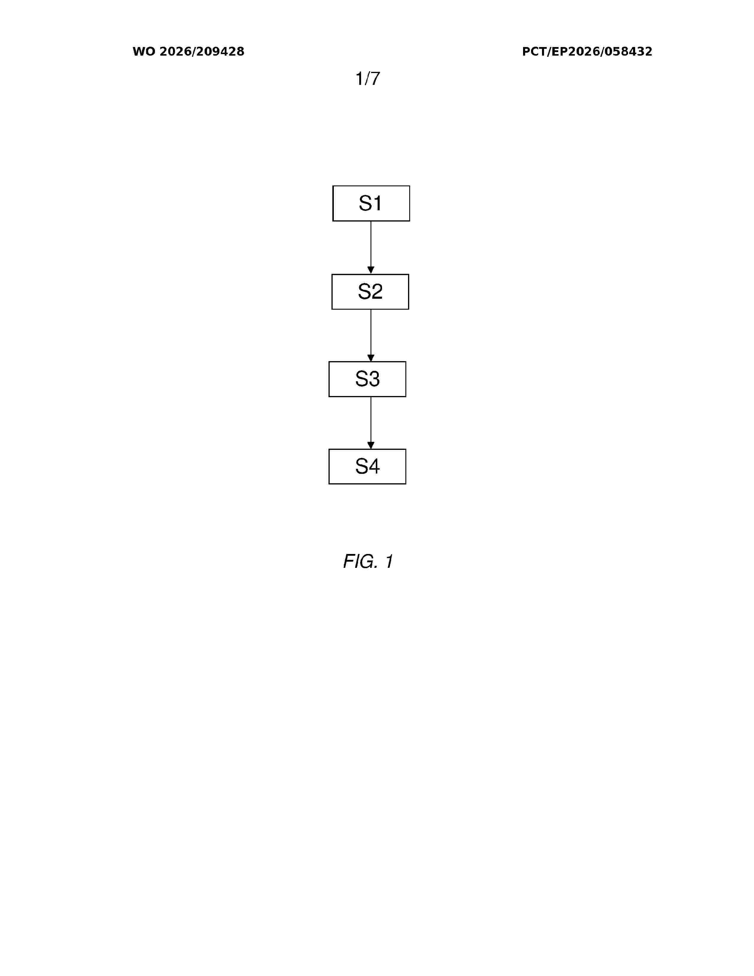
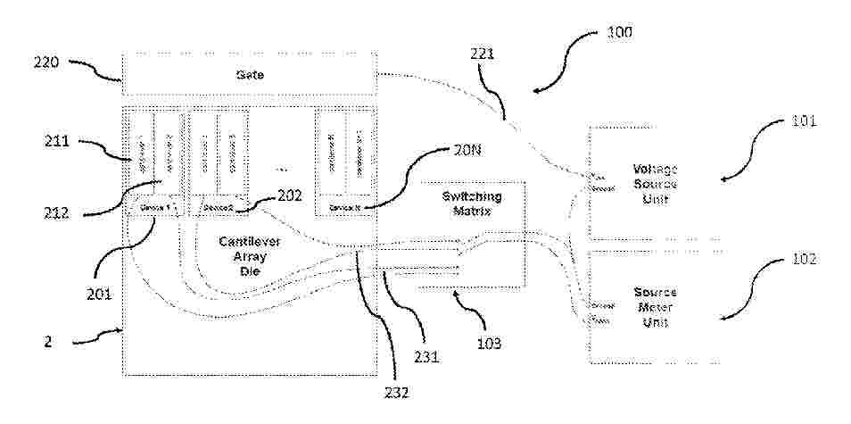
The invention relates to a method for the in situ electrical characterisation of a grown carbon nanotube connecting two neighbouring cantilevers within a cantilever chip (2) and forming a low-temperature quantum dot, comprising the steps of 1) applying a voltage between two electrically conductive areas provided respectively on the two cantilevers close to the respective ends of the nanotube, the end conductive areas of the cantilevers acting respectively as drain and source of a field-effect transistor, 2) applying a gate potential to the field-effect transistor, between a gate (220) placed close to the carbon nanotube and the end conductive area acting as source, 3) measuring the current flowing between the end conductive areas of the cantilevers, and 4) processing the current measurements and the applied gate potential.
Resumen de: EP4831262A1
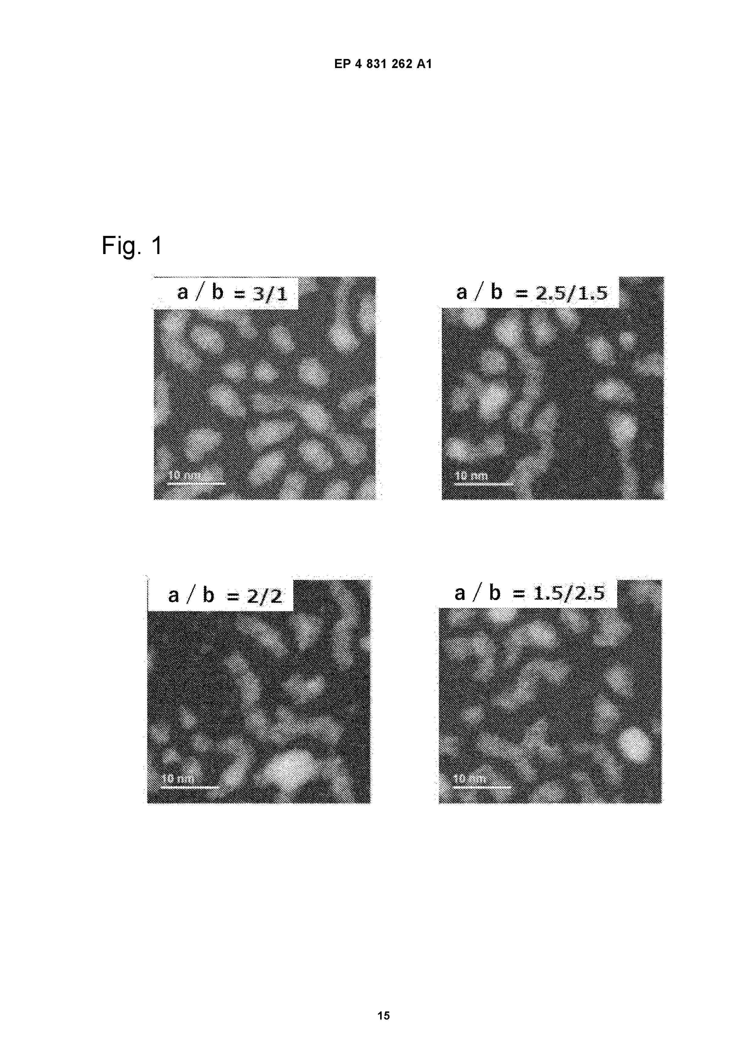
The present invention relates to a semiconductor nanoparticle including a AgCu chalcogen compound containing Ag, Cu, and a chalcogen element (Ch), represented by the following formula. In the present invention, Te is essentially contained as the chalcogen element. Te relatively large in mass among chalcogen elements is applied to allow optical response characteristics to be shifted toward a longer wavelength. The present inventive semiconductor nanoparticle includes 90% by atom or more of the AgCu chalcogen compound, in which an absorption edge wavelength on a long-wavelength side of an absorption spectrum is 1200 nm or more. Formula 1 AgxCuyChzIn the formula, Ch is a chalcogen element. x, y, and z are the respective numbers of Ag, Cu, and chalcogen element atoms, and 0.2 ≤ z/(x + y) ≤ 1 and 1.0 ≤ x/y ≤ 10.0 are satisfied.
Resumen de: EP4831351A1
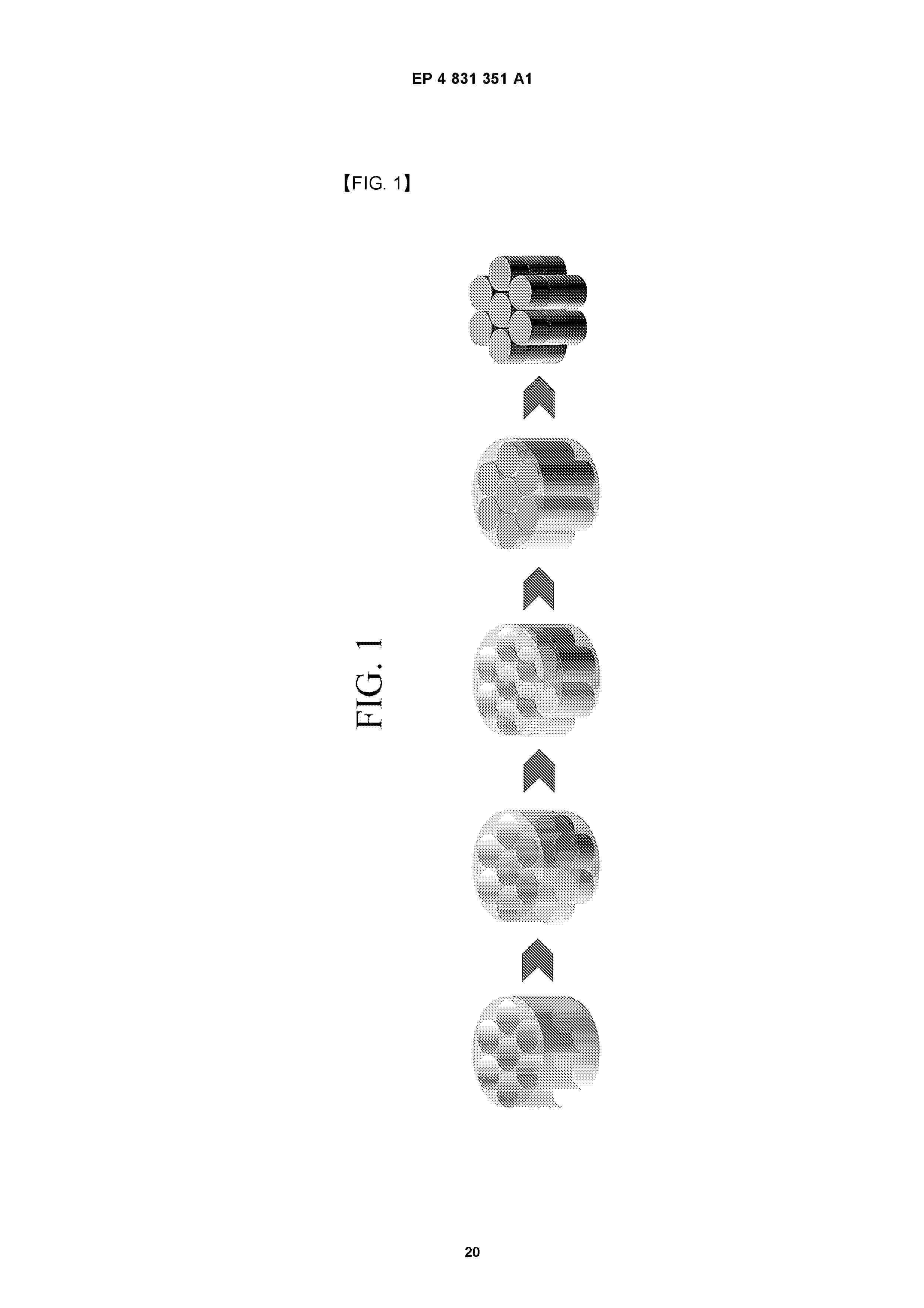
0001 The present disclosure relates to a catalyst for an oxygen evolution reaction of a water electrolysis cell, a manufacturing method therefor, a membrane-electrode assembly for a water electrolysis cell including same, and a water electrolysis cell. The catalyst for the oxygen evolution reaction of a water electrolysis cell includes a heterogeneous noble metal composite which has a nanowire shape and includes different first and second noble metal oxides in a node structure, whereby the catalyst can reduce the amount of the noble metals used while improving performance and can enhance performance and durability depending on the types and lengths of the noble metals forming the heterogeneous noble metal composite.
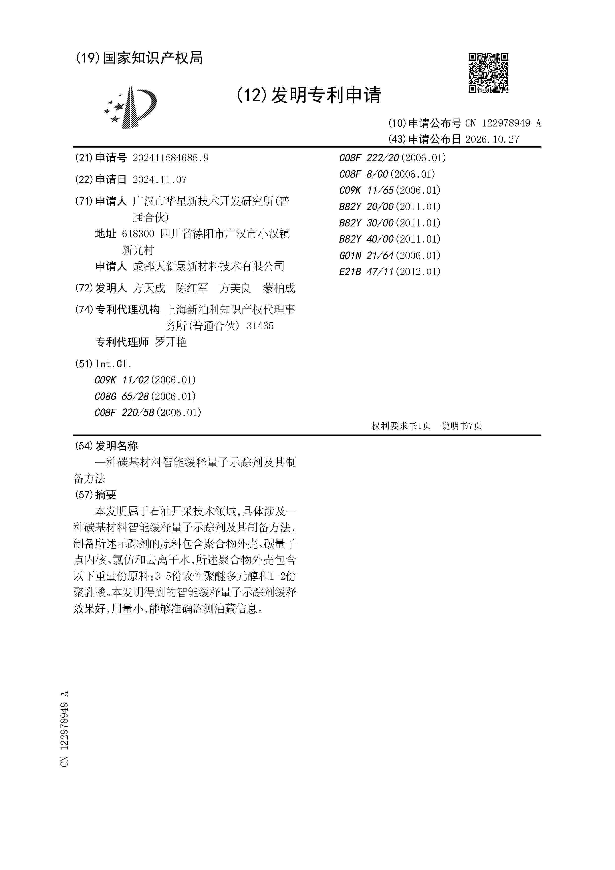
Resumen de: CN122978949A
0001 本发明属于石油开采技术领域,具体涉及一种碳基材料智能缓释量子示踪剂及其制备方法,制备所述示踪剂的原料包含聚合物外壳、碳量子点内核、氯仿和去离子水,所述聚合物外壳包含以下重量份原料:3‑5份改性聚醚多元醇和1‑2份聚乳酸。本发明得到的智能缓释量子示踪剂缓释效果好,用量小,能够准确监测油藏信息。
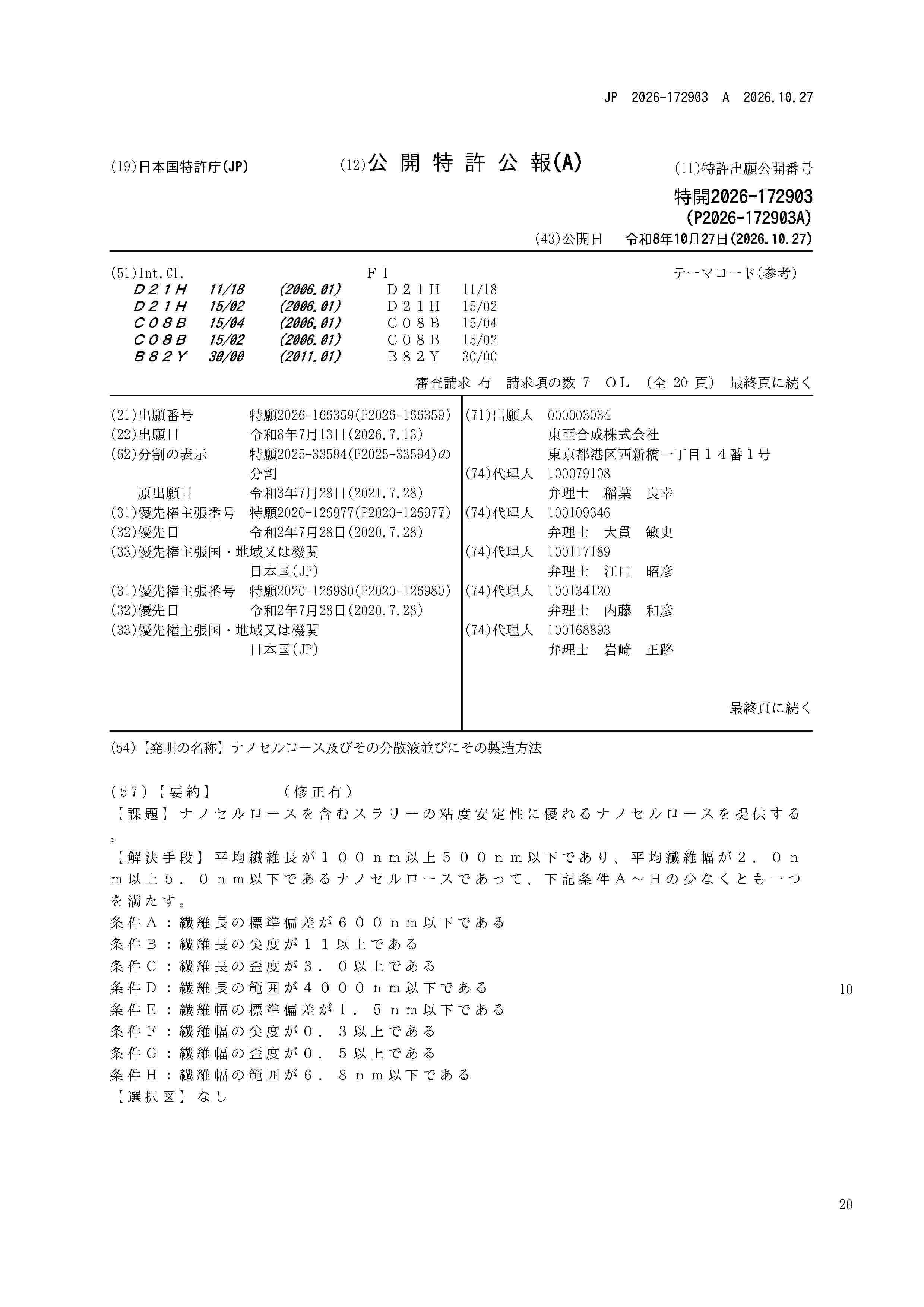
Resumen de: WO2022025100A1
The present invention provides nanocellulose that produces nanocellulose-containing slurry having stable viscosity, the nanocellulose having an average fiber length of 100-500 nm, an average fiber width of 2.0-5.0 nm, and satisfying at least one of the following conditions. Condition A: the standard deviation of the fiber length is 600 nm or less. Condition B: the kurtosis of the fiber length is 11 or greater. Condition C: the skewness of the fiber length is 3.0 or greater. Condition D: the range of the fiber length is 4000 nm or less. Condition E: the standard deviation of the fiber width is 1.5 nm or less. Condition F: the kurtosis of the fiber width is 0.3 or greater. Condition G: the skewness of the fiber width is 0.5 or greater. Condition H: the range of the fiber width is 6.8 nm or less.
Resumen de: CN122977430A
0001 本发明属于无机功能材料制备技术领域,提供了一种利用ZIF‑8晶种诱导调控锌铝水滑石的结晶方法及应用,锌铝水滑石制备方法包括以下步骤:制备ZIF‑8晶种悬浮液;配制LDH前驱体溶液;共沉淀和水热结晶;产物后处理。本发明首创性地将ZIF‑8纳米晶作为牺牲性晶种引入合成体系,通过异相成核机制精准控制水滑石结晶过程,成功制得粒径800‑900nm、分布均匀的类球状锌铝水滑石。本发明所制备的ZnAl‑LDH产品在聚氯乙烯基体中分散性极佳,在赋予材料优异热稳定性能和HCl吸收能力的同时,完美保持制品的高透明性,为高端PVC制品提供了长效稳定的抗老化新方案。
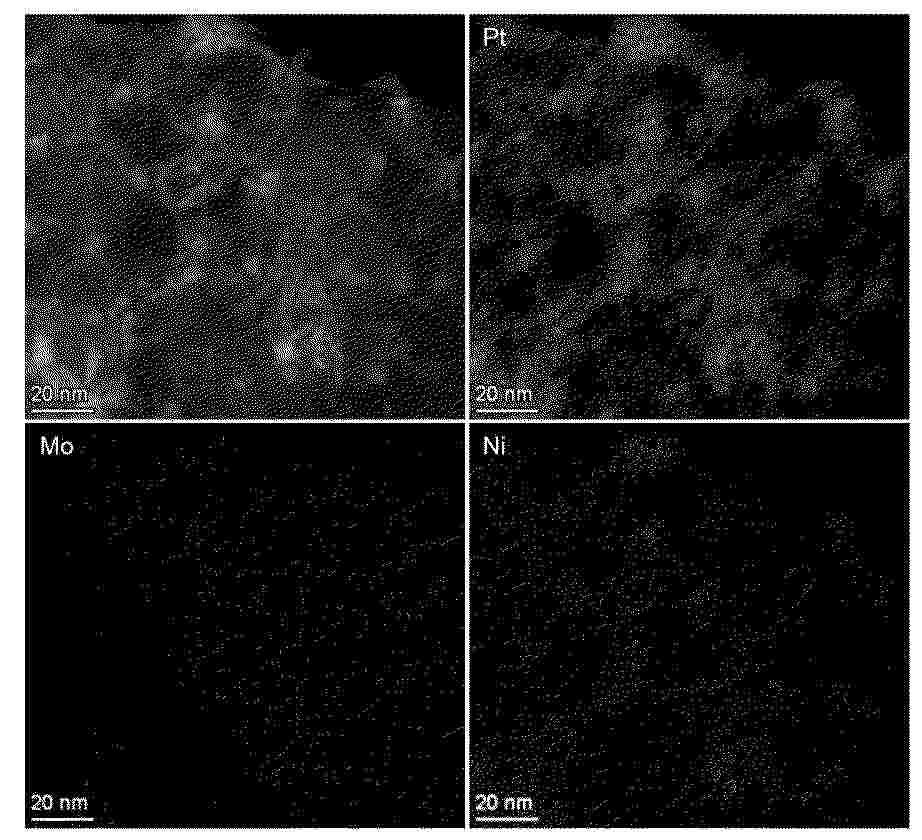
Resumen de: CN122979695A
本发明涉及电催化材料的技术领域,公开了一种铂基稀合金纳米线催化剂的制备方法及电催化应用,包括如下步骤:将铂前驱体、第二金属前驱体、第三金属前驱体、表面形貌调控剂和还原剂加入溶剂中,搅拌至溶解,得到混合前驱体溶液;将混合前驱体溶液进行还原反应,反应结束后离心,得到铂基稀合金纳米线催化剂;所述催化剂中第二金属和第三金属的掺杂质量分别为催化剂质量的3~5%;第二金属为钼,第三金属为镍、钴、铁或锌。本发明以第三过渡金属的微量掺杂实现合金化为核心,同时发挥其晶体生长取向介导作用与合金化电子调控作用,在低掺杂比例下诱导形成长程一维纳米线形貌,同时实现ORR催化活性与结构稳定性的协同提升。
Resumen de: CN122974908A
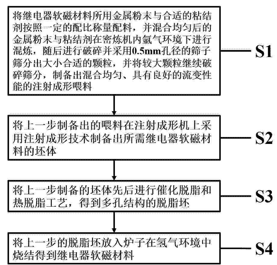
0001 本发明涉及一种粉末注射成形继电器用软磁材料的制备方法,涉及继电器软磁材料制备领域。将金属粉末与合适的粘结剂混合并在氩气环境保护下采用合适温度进行混炼,制备出混合均匀、具有良好的流变性能的注射成形喂料,再采用注射成形技术制备出所需形状继电器软磁材料的坯体。将注射坯体采用催化脱脂和热脱脂方法将粘结剂完全脱除后,在1300~1500°C的温度下烧结2~5h,得到继电器软磁材产品。本发明所制备继电器软磁材料的密度≥99%,磁感应强度B<10000>为1.6~3.0T,最大磁导率为5~25mH/m,矫顽力≤100A/m,产品尺寸精度小于±0.3%,硬度≥50HB,抗拉强度≥280MPa,延伸率≥15%。
Resumen de: WO2026221035A1
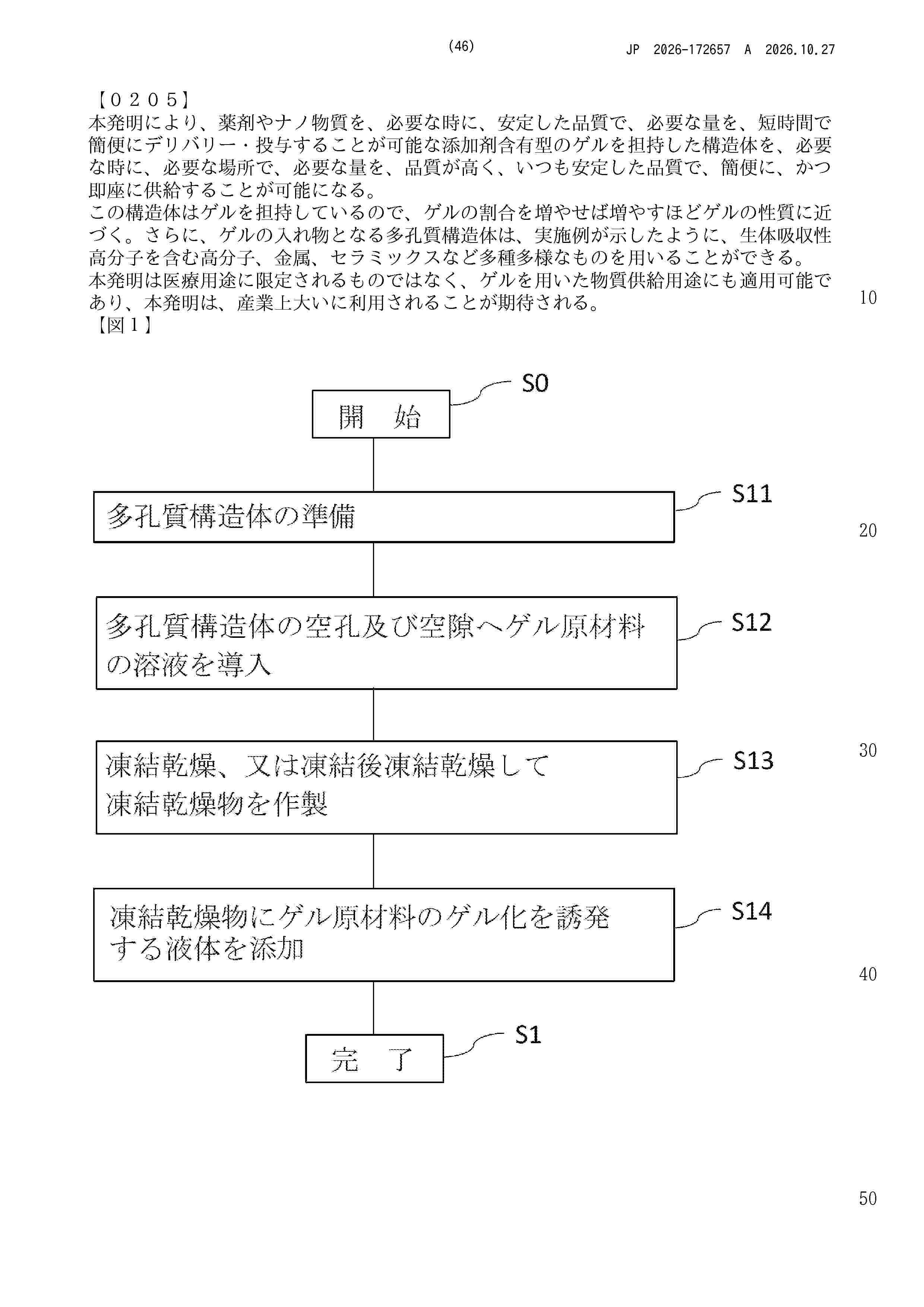
This method for producing an additive-containing gel structure includes: preparing a porous structure; introducing a solution containing a gel raw material into the internal space of the porous structure; preparing a freeze-dried product of the porous structure in which the solution containing the gel raw material is held in the internal space; and gelling the gel raw material by supplying a gelling liquid to the freeze-dried product. At least one of the solution containing the gel raw material and the gelling liquid contains one or more additives.
Resumen de: CN122977986A
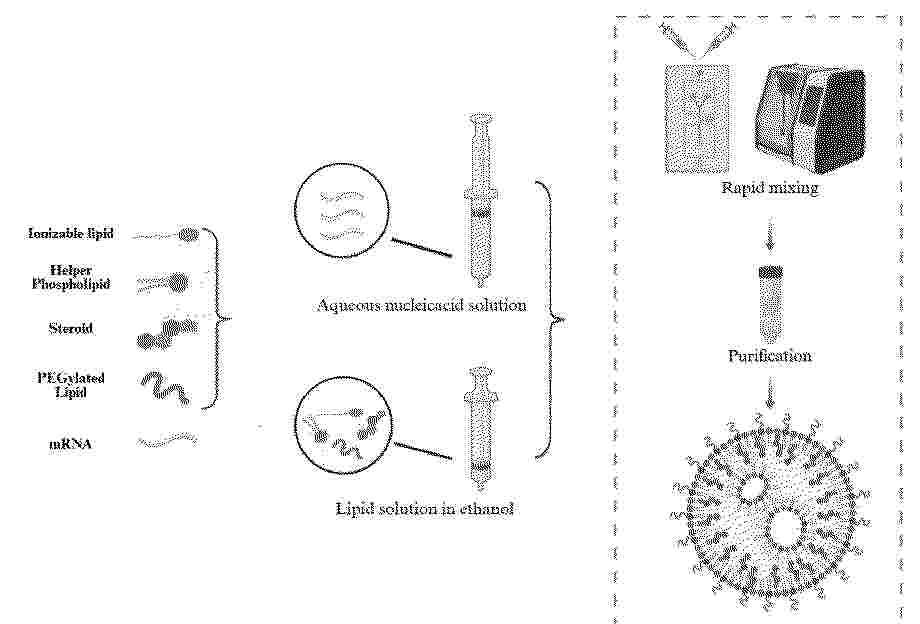
0001 本发明涉及药物递送技术领域,尤其涉及一种可电离阳离子脂质、脂质纳米颗粒及其应用。所述可电离阳离子脂质的结构式如式1N‑R、式2N‑R或式3N‑R所示。本发明的LNP包含特定结构的可电离阳离子脂质,其能与脾脏血管内皮表面蛋白结合,促进LNP外渗至脾脏实质,显著提升LNP的脾脏靶向效率。并且本发明的LNP采用可生物还原的可电离阳离子脂质,这些脂质可生物降解,在动物体内能被分解和代谢,降低了阳离子脂质相关的细胞毒性,提高了生物相容性,使药物递送过程更安全。另外,本发明的LNP还具有适用范围广、制备工艺简单稳定、粒径和电位适宜等优势,且在基因治疗、疫苗开发和肿瘤免疫治疗中具有广泛的应用前景。
Resumen de: CN122977426A
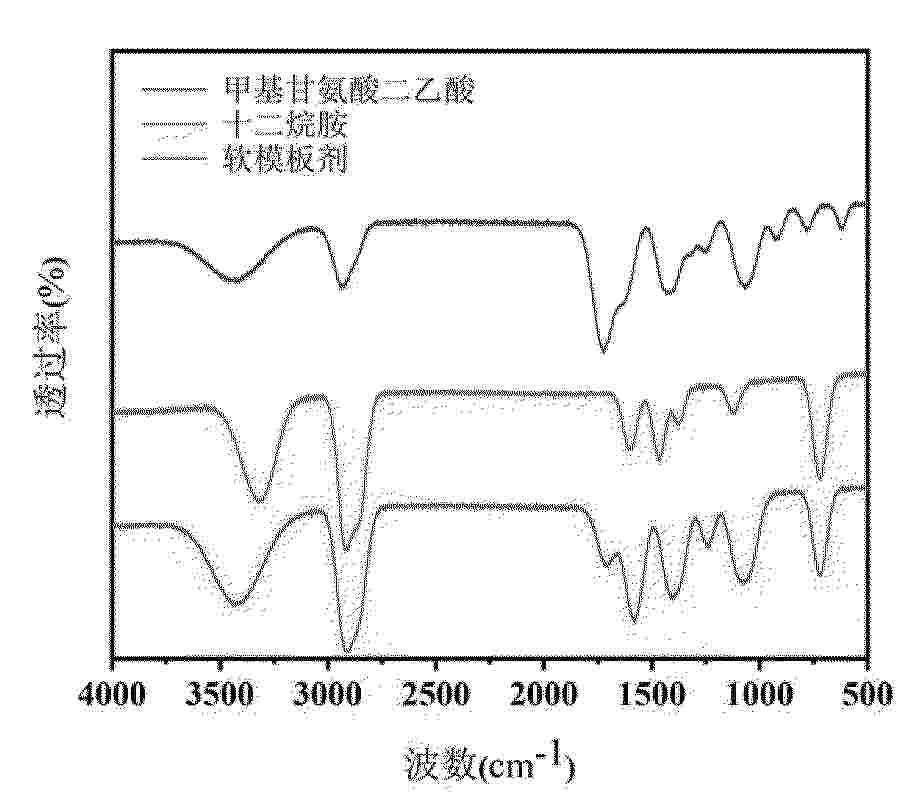
本发明公开了一种耐高温二氧化铈及其制备方法,属于稀土氧化物材料技术领域。所述耐高温二氧化铈通过以下方法制备:将铈盐溶液与软模板剂搅拌混合,使用碳酸铵水溶液调节pH至7.5‑8.5,搅拌反应,使用氨水调节pH至9‑10,经陈化、冷却、过滤、洗涤、干燥、阶梯煅烧,得到耐高温二氧化铈。本发明制备的二氧化铈具有较高的初始比表面积、良好的耐高温性能,并且可以实现粒径的可控制备。
Resumen de: CN122978134A
0001 本公开提供了一种材料体系、量子点材料及其制备方法、发光层、发光器件,该材料体系包括:第一基团,第二基团,以及连接第一基团和第二基团的连接基团;其中,第一基团包括双键或被第一保护基团保护的双键,第二基团包括巯基或被第二保护基团保护的巯基,且双键和巯基中的至少一个被保护。
Resumen de: CN122977999A
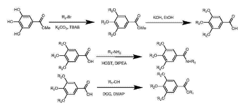
0001 本发明公开一种可电离阳离子脂质、脂质纳米颗粒及其制备方法与应用,涉及基因治疗与纳米药物递送技术领域。所述可电离阳离子脂质的结构式为:
或者
其中,R<1>为可电离叔胺基团,R<2>为饱和或不饱和烷基链。本发明的可电离阳离子脂质的结构中含有没食子酸结构和三条烷基尾链,以酯键或酰胺键连接可电离叔胺基团,其结构中含有双亚油酰链和可降解酯键,能够在肝细胞内特异性释放shRNA,通过沉默NogoB基因来抑制脂质沉积。
Resumen de: CN122992010A
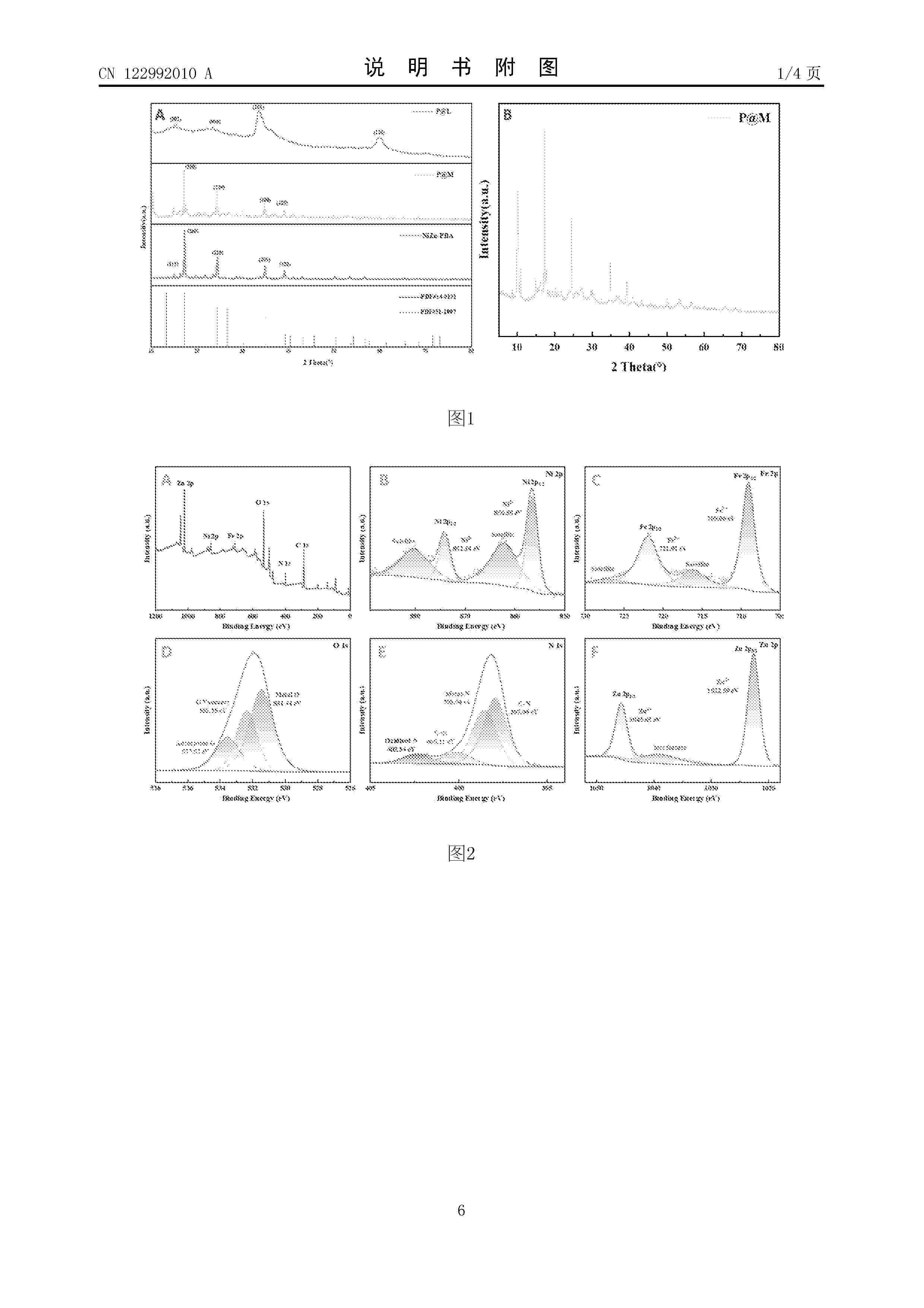
分级异质结构的构建被认为是提升电化学储能性能的有效策略。本工作通过水热生长与碱刻蚀过程构筑了一种具有三维核‑二维壳结构的NiZn‑PBA@NiZn‑LDH异质结构材料。NiZn‑PBA纳米立方体作为结构骨架,在其表面原位生长垂直交错的NiZn‑LDH纳米片,从而形成具有分级多孔结构的三维网络。该结构能够显著增加电化学活性表面积,促进电解液的快速渗透,并加速离子与电子传输动力学。结构表征结果表明该异质结构成功构筑,并伴随丰富的氧空位以及多金属氧化还原活性中心。得益于PBA核与LDH纳米片之间的协同作用,该电极表现出较高的比容量、良好的倍率性能以及优异的循环稳定性。同时,分级结构能够在充放电过程中有效缓解体积变化并保持结构稳定性。本研究为设计PBA基异质结构储能材料提供了一种有效策略。
Resumen de: CN122977333A
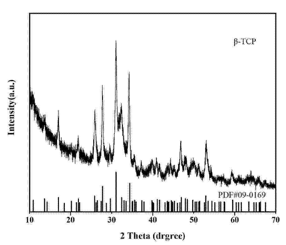
0001 本发明属于生物医用陶瓷粉体技术领域,特别涉及一种多孔纳米β‑磷酸三钙(β‑TCP)的制备方法。将钙源与有机磷源分别溶于有机溶剂,搅拌至澄清,得到钙源溶液与磷源溶液;将磷源溶液缓慢滴加至钙源溶液,边滴加边使用有机碱试剂调节体系pH 至7.0~10.0,持续搅拌得到均一前驱体溶液;将前驱体溶液转入反应釜中,160~220℃下保温10~24 h,自然冷却后得到多孔纳米 β‑TCP。本发明工艺简单、合成速度快、条件温和、产物形貌可控,避免无机杂质引入,克服了一般化学沉淀法制备样品粒径不均匀、易团聚的缺点,适合生物医用领域规模化制备。
Resumen de: CN122978950A
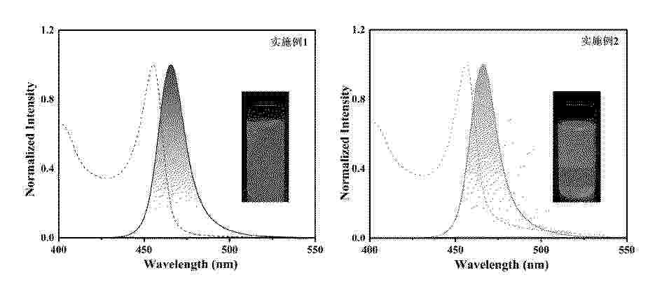
0001 本发明公开了一种对氨基苯磺酸/溴化锌协同钝化CsPbBr<3>纳米片及其制备方法和应用,属于钙钛矿发光材料技术领域。该方法包括:将碳酸铯溶于油酸中,制备油酸铯前驱体溶液;将溴化铅、油酸、油胺和对氨基苯磺酸溶于N,N‑二甲基甲酰胺中,加入油酸铯前驱体溶液,制得反应前驱体溶液,注入甲苯中反应,制得对氨基苯磺酸修饰的CsPbBr<3>纳米片分散液;纯化后,采用溴化锌后处理溶液对纳米片进行表面处理。本发明在纳米片生长过程中引入对氨基苯磺酸,并结合溴化锌后处理,实现对CsPbBr<3>纳米片表面欠配位铅离子和溴空位缺陷的协同钝化,所得材料具有蓝光发射、高光致发光量子产率和环境储存稳定性的特点。
Resumen de: CN122977372A
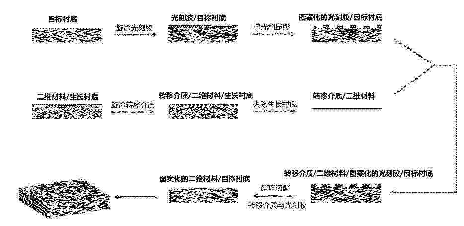
本发明涉及二维材料图案化领域,具体为一种免刻蚀图案化二维材料的方法。本发明在目标基底上旋涂光刻胶,采用传统的光刻工艺进行曝光并显影,形成特定的图案;后续将有转移介质保护的二维材料薄膜转移至图案化的光刻胶表面,对样品进行真空烘干,在去胶液中超声溶解去除图案以外区域的二维材料、光刻胶及转移介质后,即可在目标基底表面获得图案化的二维材料。本发明具有工艺简单,无需使用等离子体处理或反应离子刻蚀等刻蚀手段,可制备大面积二维材料图案及多层二维材料同质或异质结阵列等特点,为二维材料及其异质结在电子器件、光电子器件等领域的研究和应用奠定了基础。
Resumen de: CN122995545A
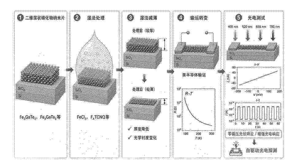
0001 本发明公开了一种定向选区湿法减薄诱导二维铁基层状碲化物光伏响应的方法及器件。所述方法以二维铁基层状碲化物纳米片为原料,使其局部区域与湿法处理剂接触,形成中间减薄、边缘不减薄的结构,使二维铁基层状碲化物纳米片发生局部厚度降低、表面形貌变化和电输运行为改变,诱导材料产生光伏响应。同时,两端未处理区域仍保持磁性金属态,外加磁场可通过调控两端磁性金属区域及其与中间半导体区域之间的载流子输运,使器件输出光电流随磁场发生变化。该方法工艺简单、条件温和、可局域图案化,适用于自驱动光电探测器、宽谱光电探测器、多波长光伏器件、低功耗光电传感器和单像素成像器件。
Nº publicación: CN122979858A 27/10/2026
Solicitante:
华东理工大学
Resumen de: CN122979858A
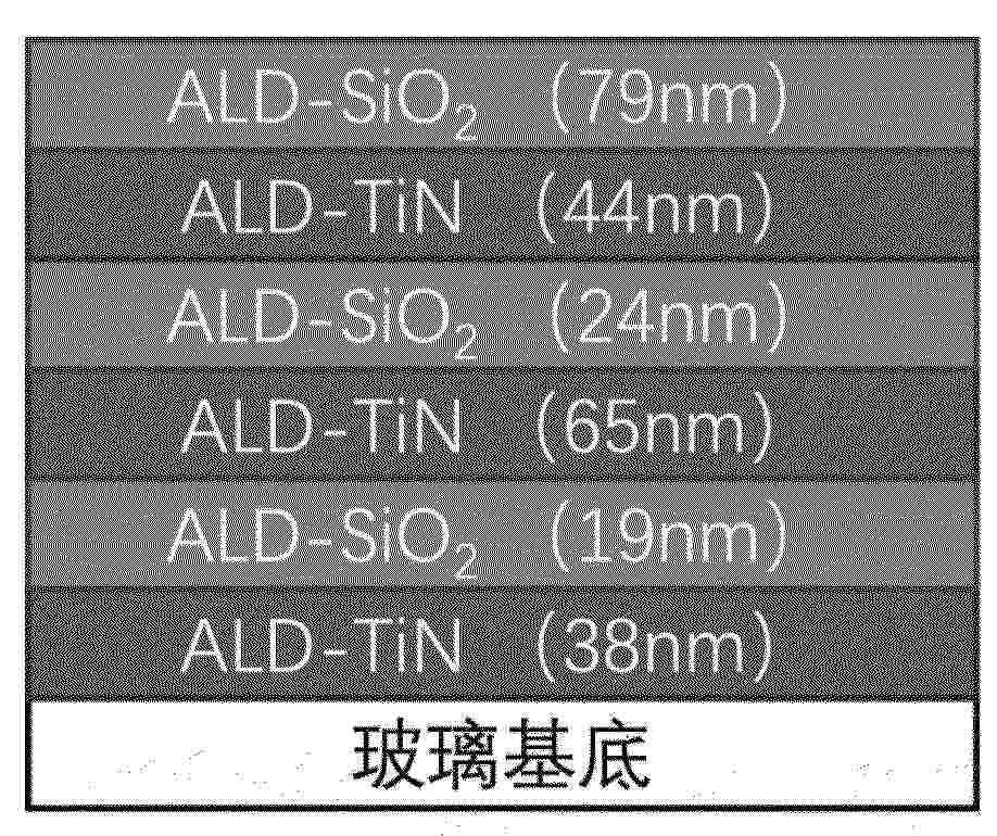
本发明公开了一种TiN/SiO2纳米叠层超低反射膜及其制备方法,属于光学薄膜制备技术领域。该方法包括:提取TiN和SiO2的光学常数,建立多层膜结构模型;以400‑700nm波段平均反射率最小化为目标,以峰值反射率低于0.5%为约束,定义峰值反射率,并以加权罚函数为优化目标进行逆向优化;采用PE‑ALD技术沉积获得多层膜结构;实测光谱后进行反向拟合修正,重复制备直至实测平均反射率低于0.2%且峰值反射率低于0.5%。制备的产品在400‑700nm波段平均反射率低于0.2%,优于ITO等传统透明导电材料;结合光学模拟全局优化与ALD亚纳米级沉积精度,避免传统试错法低效与不确定性。
 BOPI
 Sede Electrónica