

Si deseas distinguir tus productos, servicios o ambos de los de otra empresa, es posible que necesites una marca o nombre comercial. Descubre qué son, en qué consiste su procedimiento de registro y qué implica.

Información sobre los plazos de presentación de solicitudes de transformación de marcas de la Unión Europea en marca nacional española. Más información


Si tienes un nuevo dispositivo, producto o procedimiento que resuelva un problema técnico o tenga una ventaja práctica, existen distintas formas de protegerlo en España y en otros países. Descubre cómo hacerlo.

¿Tu innovación reside en la estética, la ornamentación o la apariencia de tu producto? Protégela mediante un diseño industrial. Descubre qué derechos confiere el registro y cómo realizar la tramitación.

Las indicaciones geográficas protegen el nombre de un producto originario de una zona geográfica, a la cual le debe una determinada calidad, reputación u otra característica. Descubre qué son, en qué consiste su procedimiento de registro y qué beneficios conceden.

Las patentes publicadas en todo el mundo son una valiosa fuente de información científica, técnica y comercial.

Si eres emprendedor/a o una empresa y quieres potenciar y mejorar la rentabilidad de tu negocio protegiendo de forma adecuada los activos intangibles de tu organización, en este espacio encontrarás lo necesario.


 182
resultados
182
resultados
 Última actualización
18/03/2026 [07:03:00]
Última actualización
18/03/2026 [07:03:00]


 Resultados 150 a 175 de 182

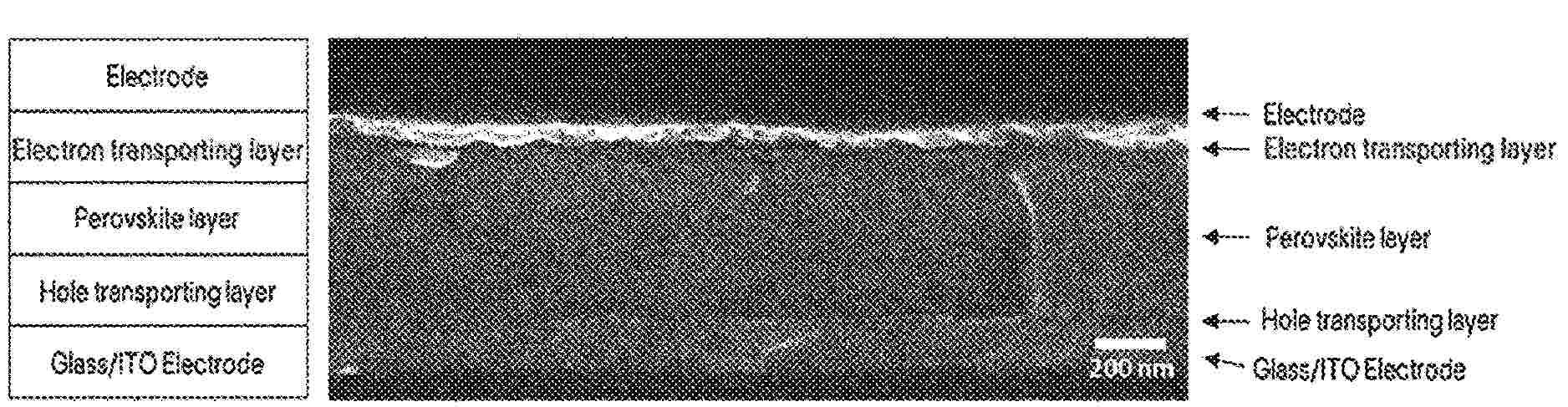
Resumen de: US20260062556A1
The present invention relates to an inverted perovskite prepared by providing a surface-modified metal oxide nanoparticle as a coating agent for forming an electron transporting layer (or electron transport layer), and using the surface-modified metal oxide nanoparticle as a coating agent prepared in a dispersion type.

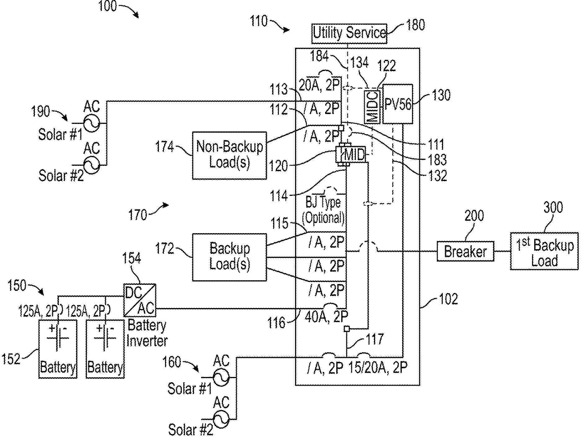
Resumen de: US20260066665A1
The present disclosure provides curtailing photovoltaic (PV) power output and autonomous load breaking in a backup mode of an electrical system. The electrical system includes a PV system, an energy storage system having a storage converter, and an energy control system. The energy control system is electrically coupled to the PV system, the energy storage system, and a plurality of backup loads. The electrical system includes an autonomous load breaker electrically coupled to a first backup load. When the energy control system switches from an on-grid mode to the backup mode, the storage converter adjusts the frequency of the power supplied to the backup side of the energy control system to a setpoint frequency that curtails PV power output, and the autonomous load breaker electrically disconnects the first backup load from the energy control system.
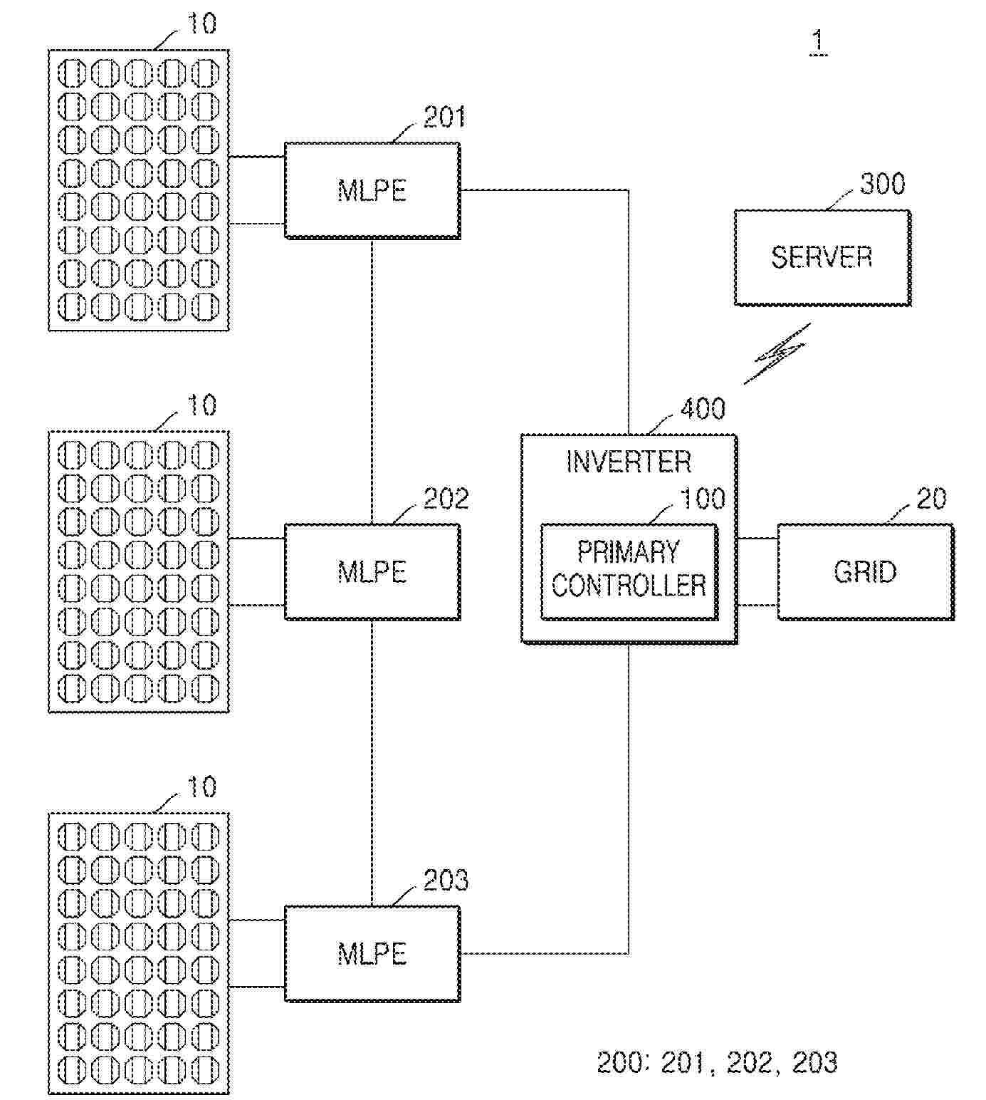
Resumen de: US20260066664A1
Provided are an inverter and a primary controller of a photovoltaic power generation system, and a method of operating the photovoltaic power generation system. The method of operating a photovoltaic power generation system may include assigning identification information to each of a plurality of module-level power electronics (MLPEs) connected to a plurality of photovoltaic panels, based on a registration request from each of the plurality of MLPEs, monitoring the plurality of MLPEs and determining whether an error has occurred in the plurality of MLPEs based on a result of the monitoring, and marking an error flag on the identification information of at least one MLPE among the plurality of MLPEs when it is determined that the error has occurred in the at least one MLPE.
Resumen de: US20260066674A1
The Smart Energy Consumption Monitoring System with Integrated Fast Charging and Solar Power provides a comprehensive solution for monitoring and managing energy usage in real-time for mobile devices. The system integrates sensors, data processing units, machine learning algorithms, solar panels, an MPPT module, and a fast-charging module to optimize energy consumption, promote efficiency, and ensure sustainable power supply.
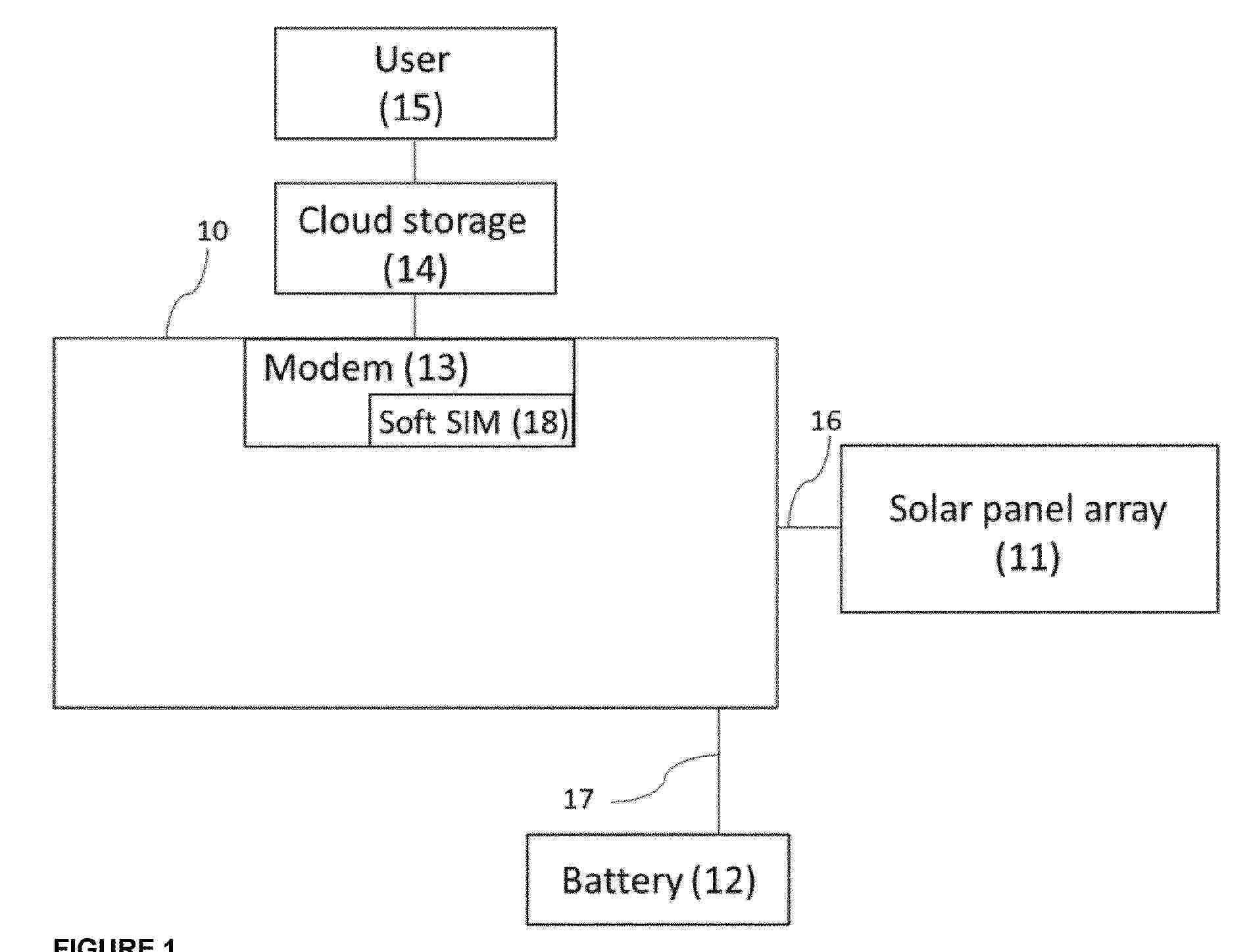
Resumen de: US20260066673A1
A solar charge controller for at least one solar panel array and at least one battery, the solar charge controller being adapted to be electrically connected with the at least one solar panel array and the at least one battery, the solar charge controller includes a built-in modem configured for two-way communication between the solar charge controller and a user, the built-in modem includes a soft SIM. A system including a plurality of solar charge controllers. A method of two-way communication between a solar charge controller and a user.
Resumen de: US20260068335A1
A solar battery according to the present embodiment has an electrode, which includes a metal and an adhesive material, formed in a conductive region including a polycrystalline semiconductor layer, and thus, the electrical characteristics of the solar battery may be improved and the manufacturing process thereof may be simplified. More specifically, the solar battery includes a semiconductor substrate, and the conductive region including the polycrystalline semiconductor layer is positioned on one surface of the semiconductor substrate.
Resumen de: US20260068507A1
Provided is a display device including: a substrate including a display area and a peripheral area that includes a bending area disposed adjacent to the display area; a plurality of pixels arranged in the display area; a driving circuit arranged in the peripheral area; a barrier rib layer arranged in the bending area; an input detection layer disposed on the plurality of pixels; and an optical functional layer including a first layer that is disposed on the input detection layer and includes a first opening in an area corresponding to the plurality of pixels, and a second layer that is disposed on the first layer and having a refractive index different from the first layer, wherein the first layer includes at least one valley located between the bending area and the driving circuit.
Resumen de: US20260066842A1
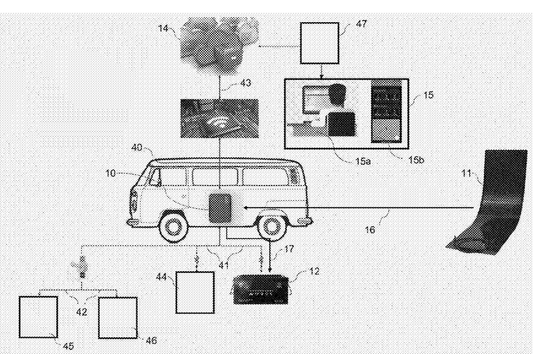
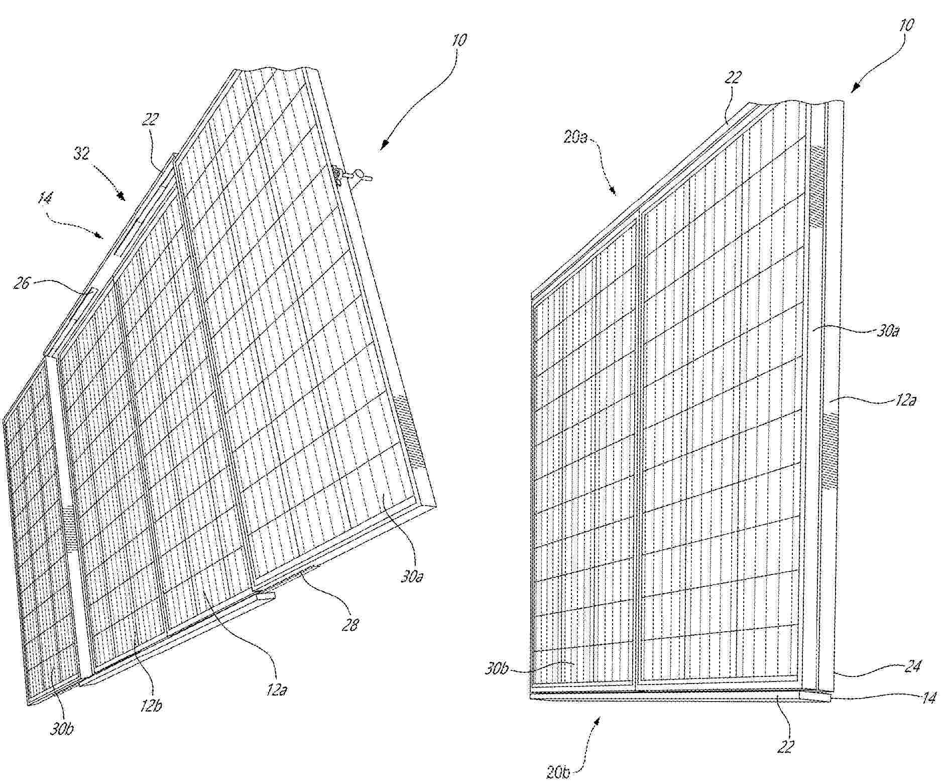
Described are various embodiments of an expandable solar panel array and a solar panel installation kit for installing at least two solar panels on a vehicle, such array and/or kit having a generally nested configuration of solar panels or structures. Some embodiments include a wire guide assembly which is configured to route electrical wiring from an upper solar panel or structure to at least partially beneath a lower solar panel or structure, so as to at least partially retain the electrical wiring during translation of the upper solar panel or structure relative to the lower solar panel or structure, thereby to avoid wiring entanglement and/or damage to the lower solar panel or structure in use.
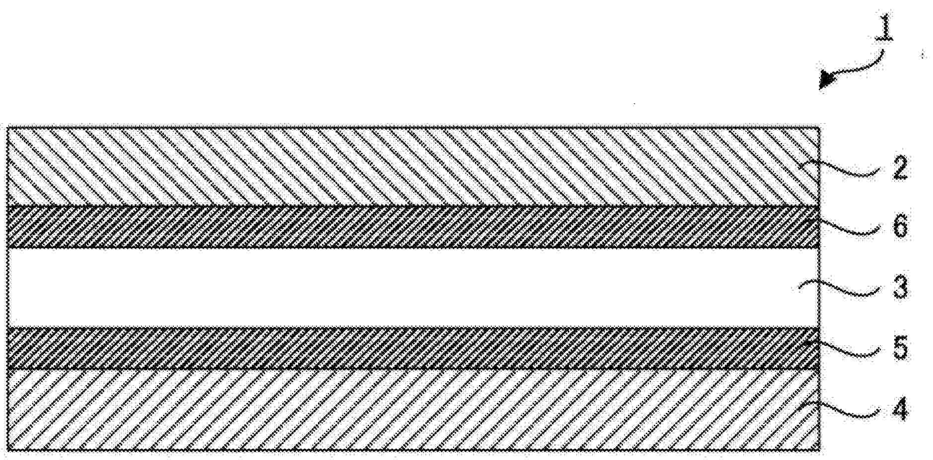
Resumen de: US20260068334A1
Provided is a solar cell module insulation film disposed between a solar cell and a steel sheet in a solar cell module, the solar cell module insulation film including: a sealing material layer, an insulating substrate, and a polyethylene-based resin layer, in this order, wherein the polyethylene-based resin layer is a polyethylene film; and a wetting tension of a surface of the polyethylene-based resin layer that is opposite side to the insulating substrate is 36 dyne/cm or more.
Resumen de: US20260066837A1
A system includes a processor that measures an angle of the sun, measures a light intensity, acquires weather information, measures a wind speed, receives data obtained from the foregoing measurements and acquisitions, analyzes the data, generates a control command to optimally adjust an orientation, angle, and area of a solar panel based on a result of analyzing the data, and physically adjusts the solar panel based on the control command.
Resumen de: US20260066846A1
A vehicle includes a solar panel that is provided on a top portion of a vehicle body, and a protruding portion that is provided forward of the solar panel on the vehicle body. The protruding portion has a shape that is tapered forward in a front-rear direction of the vehicle body.
Resumen de: US20260066843A1
A cover attachment structure partially covers a solar panel unit including a solar panel and a frame from outside with a cover. A cover receiving member receives, from below, the frame supporting the solar panel, with a receiving portion at an end thereof closer to inside with respect to an inside-outside direction. A cover hold down member holds down the frame from above with a hold down portion at an end thereof closer to the inside with respect to the inside-outside direction. The cover is attached to the solar panel unit with the cover receiving member and the cover hold down member. The cover hold down member is placed on the cover such that a length from the receiving portion to the hold down portion is adjustable.
Resumen de: US20260048287A1
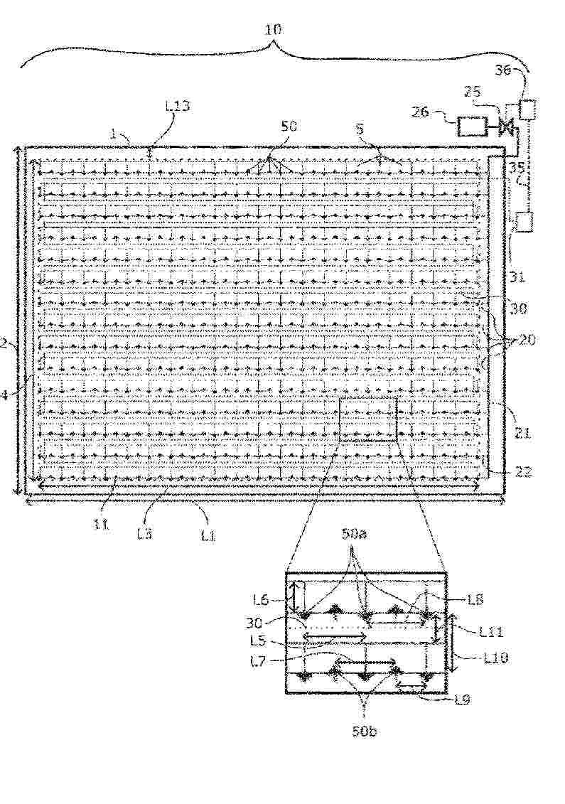
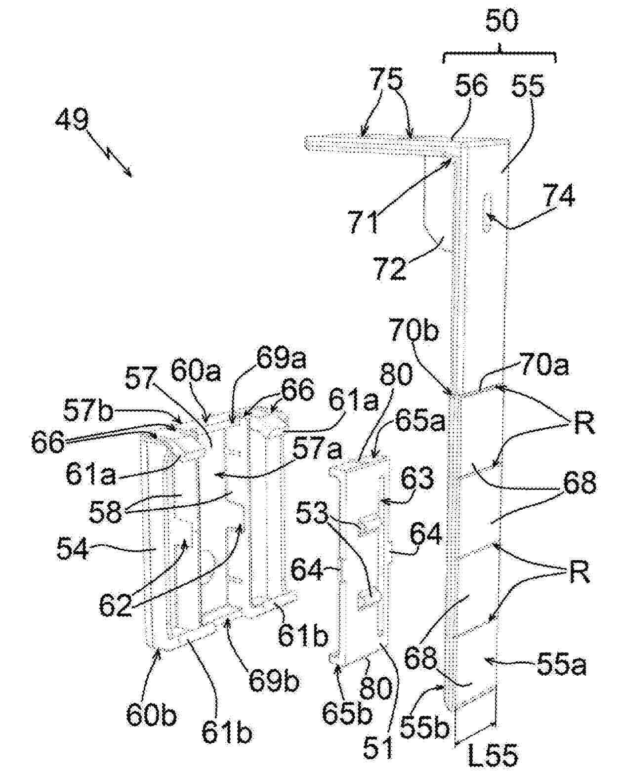
Fire protection systems for a rooftop solar panel installation with solar panels. The fire protection system has a group of water spray nozzles with a metric K-factor of 20 or less to discharge firefighting fluid to a coverage area of the rooftop solar panel installation, a fluid pipe system connecting the group of water spray nozzles to a fluid supply for providing firefighting fluid, a fire hazard detection system with at least one fire hazard detector configured to monitor the coverage area, and at least one detection control unit to generate an alarm signal upon detection of a fire hazard within the coverage area, a valve unit configured to control passage of the firefighting fluid from the fluid supply, wherein the coverage area is at least 500 m2, and the group of water spray nozzles is configured to discharge the firefighting fluid received from the fluid supply to the coverage area with a normalized fluid application rate of 15 mm/m2/min or less.
Resumen de: US20260066836A1
An electrical power supply device comprises a casing, a photovoltaic panel, which is fixed on the casing, and a fixing device, which comprises a fixing support, a holding device and a cover. The support comprises a plurality of first locking elements. The holding device comprises at least one second locking element, which cooperates with one of the first locking elements. The holding device is fixed on the cover. The cover is fixed removably on the casing. Furthermore, the support is arranged between the casing and the cover, so as, on the one hand, to be able to slide the support between the casing and the cover and, on the other hand, to hold the support in position by the holding device.
Resumen de: US20260066675A1
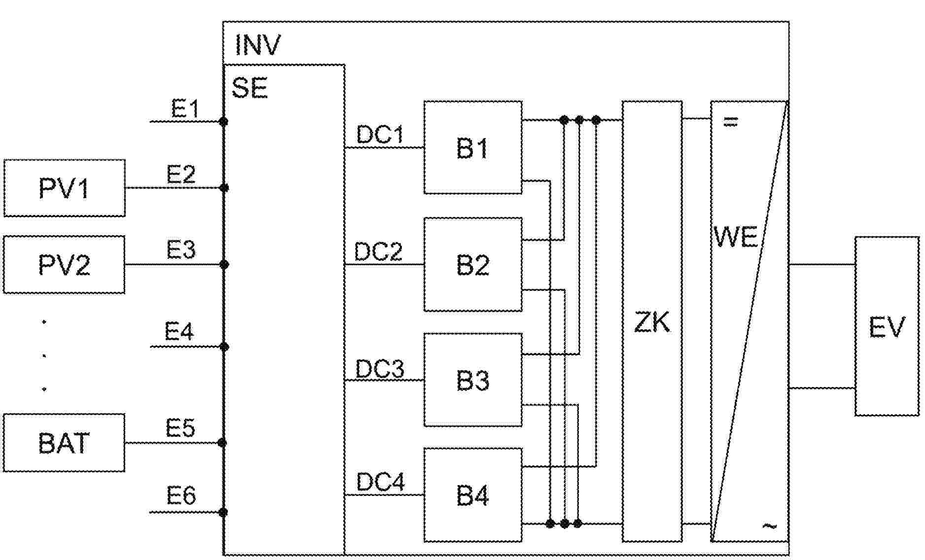
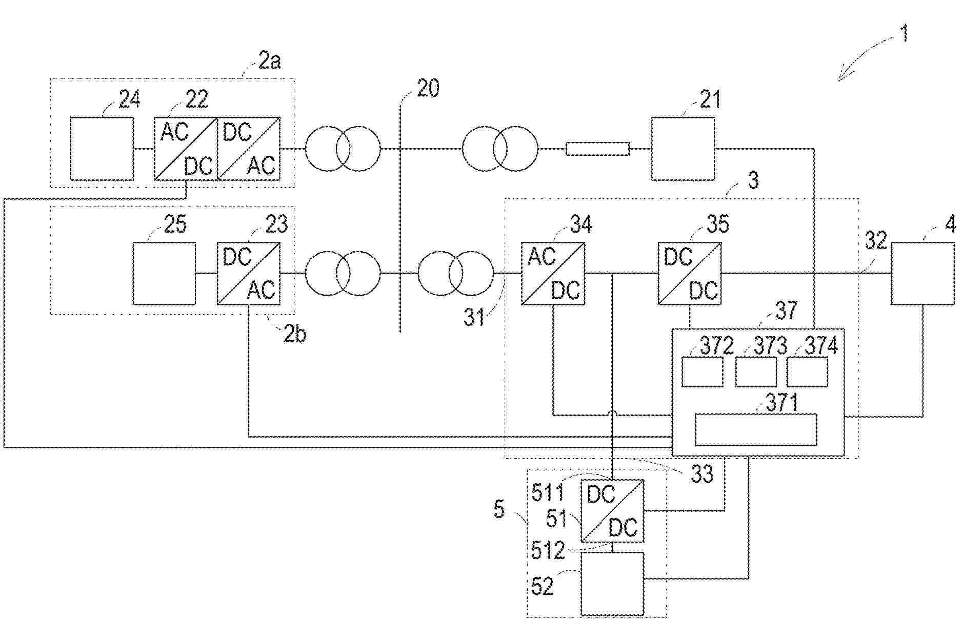
The present invention relates to an inverter system (INV) for a photovoltaic system and to a method for operating the inverter system (INV). The inverter system (INV) comprises an inverter unit (WE), ), to which a predetermined number of DC-to-DC converters (B1, . . . , B4) is connected upstream via an intermediate circuit (ZK). The DC inputs (DC1, . . . , DC4) of the inverter system (INV) are formed by the DC-to-DC converters (B1, . . . , B4), which predetermines the number and properties of the DC inputs (DC1, . . . , DC4). The DC inputs (DC1, . . . , DC4) are connected to different direct-voltage units (PV1, PV2, BAT, EC, GE, VB), in particular PV units, energy storage units, etc. A switching unit (SE), which comprises inputs (E1, . . . , E6) for connecting the direct-voltage units (PV1, PV2, BAT, EC, GE, VB), is connected to the DC inputs (DC1, . . . , DC4). The switching unit (SE) is thus arranged between the DC-to-DC converters (B1, . . . , B4) forming the DC inputs (DC1, . . . , DC4) and the direct-voltage units (PV1, PV2, BAT, EC, GE, VB) which are connectable to the switching unit (SE). The different direct-voltage units (PV1, PV2, BAT, EC, GE, VB) connected to the inputs (E1, . . . , E6) are identified (101, 102), and for each direct-voltage unit (PV1, PV2, BAT, EC, GE, VB) connected to an input (E1, . . . , E6) of the switching unit (SE) a current value of at least one power variable is determined (103). The determined current value of the at least one power variab
Resumen de: US20260066663A1
A power supply system includes at least four direct current converters and an inverter. The inverter includes at least two DC/DC circuits. The inverter controls an input end of one DC/DC circuit in the at least two DC/DC circuits to be short-circuited. The at least four direct current converters detect, in response to a case in which the input end of the DC/DC circuit in the at least two DC/DC circuits is short-circuited, whether output operating parameters of the at least four direct current converters meet a preset operating parameter range, and set a number for a direct current converter that is in the at least four direct current converters and whose output operating parameter meets the preset operating parameter range.
Resumen de: US20260066662A1
A power system and a control method of the power system are provided. The power system determines the operating mode according to the states and parameters of one or more of the power sources, the energy storage device and the hydrogen generation device. The power source and the corresponding power transmission path for hydrogen generation is selected. The selected power source supplies power. The selected power is converted and transmitted to provide the electric power required by the hydrogen generation device through the selected power transmission path. The selected optimal power source and the power transmission path supply power to the hydrogen generation device with stable, continuous, enhanced efficiency and reduced cost.
Resumen de: US20260068333A1
The present application relates to a conductive component, a solar cell string, and a photovoltaic module. An outer periphery of the conductive component is defined with a plurality of welding regions and a plurality of adhesive bonding region. The welding regions and the adhesive bonding regions are arranged alternately in a first direction. The outer periphery of the conductive component is provided with a plurality of flux parts respectively corresponding to the plurality of welding regions. Each of the flux parts is at least partially coated, along a perimetral direction of the conductive component, on the conductive component in a corresponding one of the welding regions.
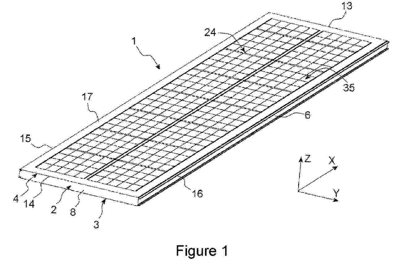
Resumen de: WO2026047377A1
The invention relates to a process for manufacturing a sandwich panel comprising a photovoltaic active area positioned on the outer sheet and whose upper, respectively lower, electrical conductor is connected to an upper, respectively lower, cable at the backside of the outer sheet, the latter comprising a cavity in which one of the first upper electrical connector and the first lower electrical connector is positioned, the process comprising positioning the outer sheet in a mold, inserting the other of the first upper electrical connector and the first lower electrical connector, with a downstream portion of its cable, either in a hole in one of the sides of the mold or in a groove formed in the inner sheet or in a groove formed in the outer sheet, putting insulation in place and maintaining the inner sheet at a given distance from the outer sheet.
Resumen de: WO2026047378A1
The invention relates to a process for manufacturing a sandwich panel comprising a photovoltaic active area positioned on the outer sheet and whose upper, respectively lower, electrical conductor is connected to an upper, respectively lower, cable at the backside of the outer sheet, the process comprising positioning the outer sheet in a mold, inserting at least one of the first upper electrical connector and the first lower electrical connector, with a downstream portion of its cable, in a groove formed in the outer sheet, putting insulation in place and maintaining the inner sheet at a given distance from the outer sheet.
Resumen de: WO2026047370A1
The invention relates to a sandwich panel comprising a photovoltaic active area positioned on an outer sheet comprising an outer mortise and an outer tenon, the upper, respectively lower, electrical connector of the photovoltaic active area being positioned in an upper, respectively lower, cavity, the upper cavity being positioned within the insulation material in the upper half of the sandwich panel and adjacent to either one of the longitudinal sides of the insulation material or the inner sheet so that the upper electrical connector can be accessed from the upper cavity, the lower cavity being positioned within the insulation material in the lower half of the sandwich panel and adjacent to either one of the longitudinal sides of the insulation material or the inner sheet so that the first lower electrical connector can be accessed from the lower cavity.
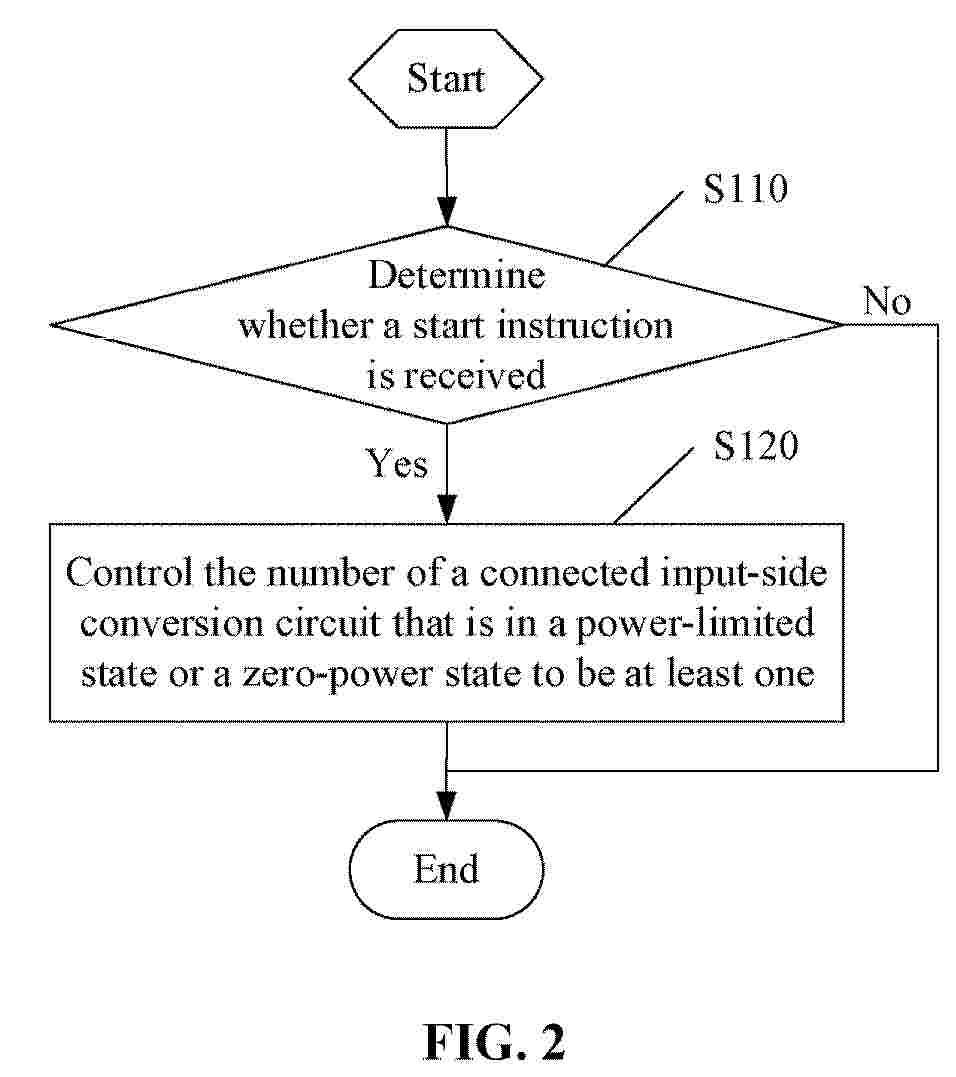
Resumen de: EP4704322A1
The present application provides a power converter and a starting method therefor. The starting method comprises after a starting instruction is received, at each moment, enabling at least one target input-side conversion circuit to be in a power-limited state or a zero-power state, wherein when the target input-side conversion circuit is in the power-limited state or the zero-power state, the input voltage of the target input-side conversion circuit is not lowered. Therefore, the input voltage of at least one target input-side conversion circuit is not lowered at each moment, that is, decoupling of power supply of a controller and power conversion of the power converter is realized, so that the starting method can avoid the problem of undervoltage shutdown of the controller, and can further avoid the starting hiccup phenomenon of the power converter. Additionally, because the power converter can be a photovoltaic inverter, the starting method can also avoid the starting hiccup phenomenon of the photovoltaic inverter.
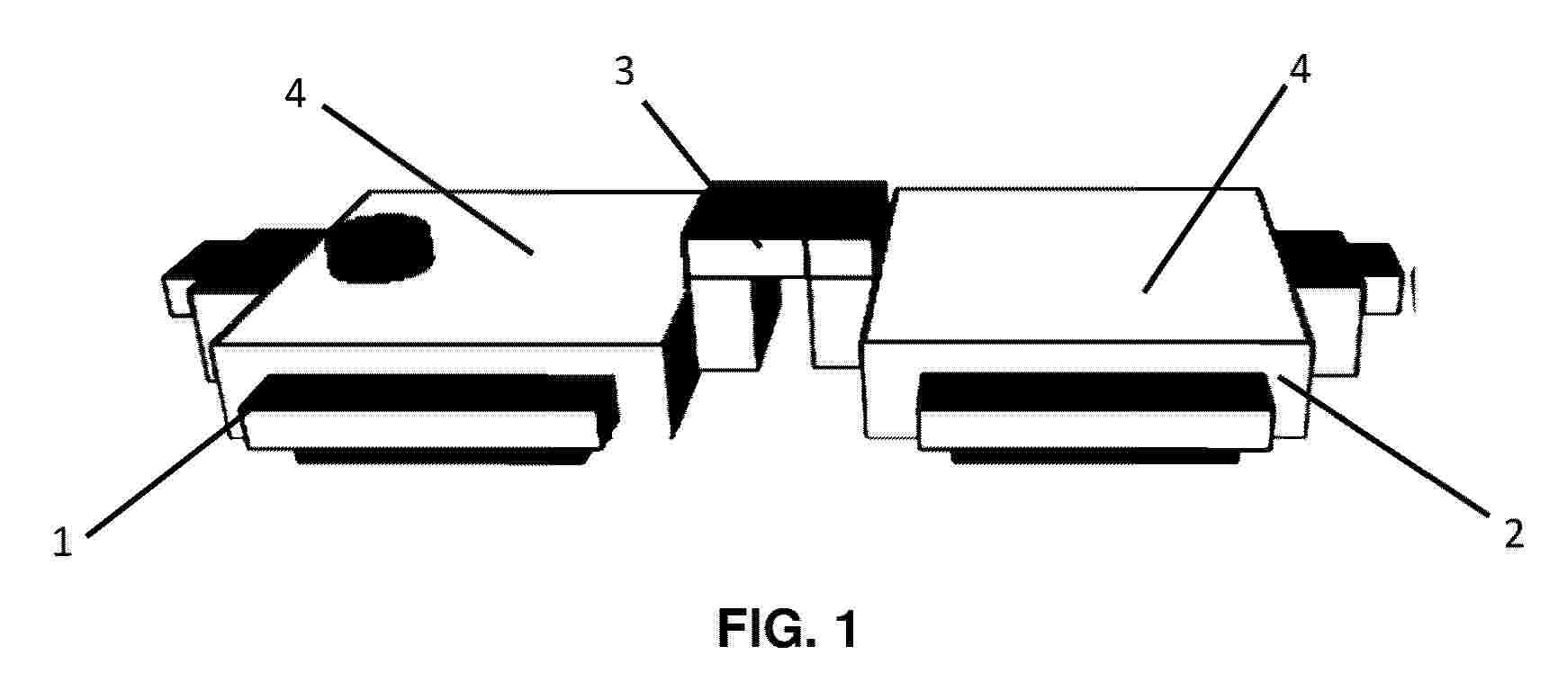
Resumen de: EP4702901A1
Glass cleaning robot, that comprises a first independent glass cleaning robot (1), a second independent glass cleaning robot (2), and a central system configured to precisely coordinate the actions of the two independent glass cleaning robots transforming them into a single, more efficient operating entity, such the central system comprises a first linear actuator (5) attached to the first independent glass cleaning robot, a second linear actuator (6) attached to the second independent glass cleaning robot, and a third linear actuator (7) attached at one end to the first linear actuator (5) and at the other end to the second linear actuator (6), where the third linear actuator (7) is perpendicular to the first linear actuator (5) and to the second linear actuator (6).
Resumen de: EP4704299A1
A solar charge controller for at least one solar panel array and at least one battery, the solar charge controller being adapted to be electrically connected with the at least one solar panel array and the at least one battery, the solar charge controller includes a built-in modem configured for two-way communication between the solar charge controller and a user, the built-in modem includes a soft SIM. A system including a plurality of solar charge controllers. A method of two-way communication between a solar charge controller and a user.
Nº publicación: EP4704334A1 04/03/2026
Solicitante:
SIEMENS SCHWEIZ AG [CH]
Siemens Schweiz AG
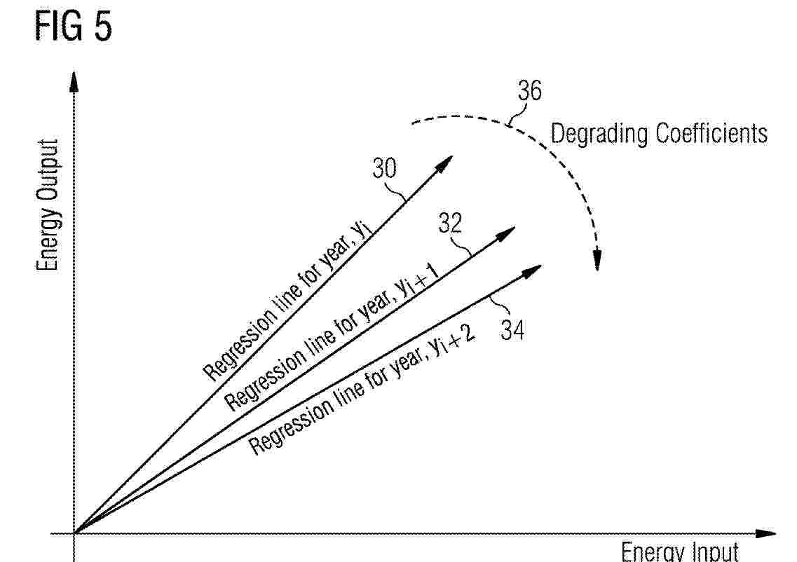
Resumen de: EP4704334A1
The invention relates to a computer-implemented method (100) for calculating an efficiency degradation rate of an energy conversion device (50) from measurement data (10) of the energy conversion device (50). The method comprises the steps of: a) providing first measurement data (14) of a first observation obtained at a first time point, the first measurement data including multiple measurement data points each relating an energy input value of the energy conversion device (50) to an energy output value of the energy conversion device (50); b) applying a mathematical model to the first measurement data (14) to obtain a function modelling the first measurement data (14); c) determining (130) a first coefficient of conversion from the obtained function, wherein the first coefficient of conversion represents a ratio of the energy input to the energy output at the first time; d) repeating (140) steps a) to c) with second measurement data of the energy conversion device (50) obtained at a second time point, the second time point being different than the first time point, thereby obtaining a second coefficient of conversion representing a ratio of the energy input to the energy output at the second time point; e) comparing (150) the first coefficient of conversion with the second coefficient of conversion to determine the efficiency degradation rate of the energy conversion device (50).
 BOPI
BOPI
 Sede Electrónica